Frontplane

Solus Advanced Materials to start supplying HTL materials to LG Display

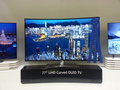
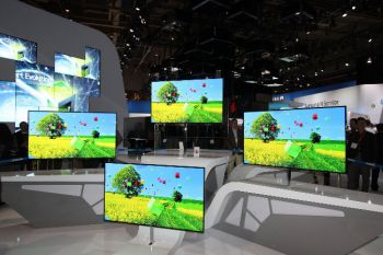
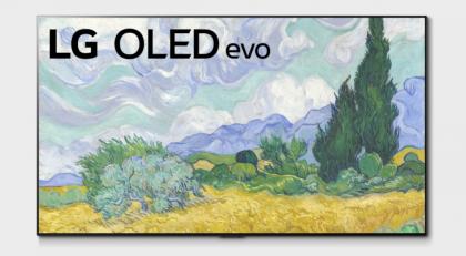
Korea-based OLED materials maker Solus Advanced Materials (previously Doosan Solus) announced that the company will start supplying HTL materials for LG Display, for its E3 line in Paju, used to produce OLED TVs.

According to reports from Korea, up until now Merck was LGD's sole HTL supplier (for large-area WOLED production), and Solus will now replace some of the HTL materials previously supplied by Merck. Solus hopes to expand shipments to LGD and supply HTL materials for LGD's other large-area WOLED fabs.

Read the full story Posted: Jun 16,2021

Doosan Solus develops ETL materials for SDC's QD-OLED stack

In 2019, Doosan Corp spun-off its OLED materials unit, which is now called Doosan Solus (and is listed on the Korean stock market). The company's main OLED products are host materials and EIL and ETL layers.

According to The Elec in Korea, Doosan Solus currently produces so called "advanced" Electron Transporting Layer (aETL) for SDC's mobile AMOLED stack, and the company is now developing specialized aETL to be adopted by Samsung in its QD-OLED stack. Solus has been the exclusive supplier of ETL mateirals for SDC for the past eight years, and its materials are adopted in Samsung's latest M11 AMOLED stack.

Read the full story Posted: Feb 18,2021

LG aims to start producing solution-based OLED panels in 2018

DisplayCentral posted an interesting article on LG Display's OLED TV program. The author reports from a discussion he had with Changho Oh, Senior VP for LG Display’s OLED TV Development Division, in which Changho says that LGD is investing heavily in soluble OLED production and aims to have such panels available in 2018.

A few days ago we reported that an LG Display researcher revealed that the company is developing a roll-to-roll process to produce flexible OLED displays. This is one of several possible printing technologies that can make soluble OLED panels possible.

Read the full story Posted: Nov 16,2014

Kateeva finally unveil their YIELDjet OLED TV inkjet printing system

Kateeva is a US based startup that was established in 2009 to develop OLED ink-jet deposition technology originally developed at MIT. The company has been been in stealth-mode for years, and now finally they have unveiled their technology and system, branded YIELDJet.

So YIELDJET is an inkjet printing system that can be used to produce OLEDs in high volume. Kateeva claims that their system, the first one engineered from the ground up for OLED mass production, will dramatically improve yields and drive production costs lower. Kateeva says that this was achieved by three major technical breakthroughs: is features a production-worthy pure nitrogen process chamber, which doubles the lifetime in certain applications, it reduces particles by as much as 10X thanks to a specialized mechanical design and it offers exceptional film coating uniformity with a process window that’s 5X wider than standard technologies.

Read the full story Posted: Nov 20,2013

Fujifilm and imec developed new photoresist-based OLED patterning technology

Fujifilm and imec have jointly developed a new photoresist-based OLED (and other organic semiconductors) patterning technology that can enable sub-micron patterns. The new process uses existing i-line photolithography equipment and may be a cost-effective production method for high resolution devices.

Photoresist technologies are based on photo-sensitive materials that cause photochemical reaction when exposed to light. This technology is already used for microfabrication in semiconductor production. The new process builds on Fujifilm's synthetic-organic chemistry material design technology.

Read the full story Posted: Sep 29,2013

Technical updates on Samsung's flexible OLED program

Samsung is getting ready to release flexible OLEDs soon, and have announced that these displays will be branded as YOUM displays. Today the OLED association released some interesting information regarding Samsung's flexible OLED manufacturing program. According to this report, products that use these displays will be introduced in Q4 2012, while mass production will begin as early as next month.

Back in May 2011 Samsung announced a joint venture with Japan's Ube Kosan to develop and produce polyimide resin - to be used as substrates for their flexible displays in a $18 million investment. Now we hear that the curing equipment for the hardened polyimide will be provided by Korea's Tera Semicon.

Read the full story Posted: Apr 11,2012

11 arrested in Korea over AMOLED technology leak from Samsung to "local rival"

The Korean police announced today that they are investigating a case of key technology leaking from Samsung Mobile Display to a local rival firm. This technology is Samsung's Small Mask Scanning, used to produce AMOLED on large substrates. The local rival may be LG Display (Samsung's biggest AMOLED competitor) but this is strange as they are using a completely different front plane architecture (WOLED-CF) in their own large panel production and this technology does not require fine patterning.

11 people were arrested in the case - former and current researchers at SMD and employees of the rival firm. The main suspect is a 46 years old former researcher at SMD who now works at the rival company. The police suspects he received 190 million Won (about $168,000) for the secret data. He is also suspect of sharing the information with a Chinese display maker.

Read the full story Posted: Apr 05,2012

OFT Edge - a new OLED deposition system by VG Scienta

VG Scienta announced a new OLED deposition system, the OFT EDGE. The OFT (Organic Flexible Transparent) system can be used to deposit and analyse organic and inorganic layers on flexible and solid substrate.

The OFT Edge technology provides low temperature deposition of TCO, metals, small molecule deposition for organics, and an interchangeable modular construction with a wide selection of both deposition and analytical tools that can be attached to the systems to further increase the flexibility of the tool. VG Scienta offers ALD modules, XPS/UPS modules, STM, IR, and AFM modules. Modules within the system can be used as either standalone units when combined with a fast entry load lock or can be fully integrated into the multi-purpose cluster tool in conjunction with a central handler.

Read the full story Posted: Feb 16,2012

Rolith develops low cost large area nanopatterning technology

Rolith says they are developing a new proprietary nanolithography technology that uses its "Rolling Mask" lithography system (RML). Rolith says that the new technology will enable low cost, high throughput and large area nanopatterning, and is suitable for OLED panels. In fact the company is seeking collaboration with companies - to jointly develop this technology.

Rolith's technology is based on a novel concept of continuous (conveyor, or Roll-to-Roll) nano patterning using cylindrical photomasks. A prototype was designed and built in 2011 in partnership with SUSS Microtec which allows patterning a 300 mm x 300 mm plates or 12 wafers. Rolith has successfully demonstrated printing dense nanostructures with less than 300 nm features, and are currently working on enhancing the resolution. The company's roadmap promises scaling up to 1m substrates in 2012 and up to 3 meters in the next 2 years. They are also developing a technology that will handle flexible substrates.

Read the full story Posted: Feb 12,2012

Jusung developed a MOCVD IGZO TFT Process

Jusung Engineering reports that they managed to developed a a new metal organic chemical vapor deposition (MOCVD) technology to apply IGZO for use on flat panels. Jusung says they are the only company to develop an 8-Gen MOCVD IGZO tool, and that this technology will be compatible with future OLED display processes. We talked to Jusung and they say that they are already in talks with several potential clients (in Japan, China and Korea) and they hope to get purchase orders and start shipping equipment in the middle of 2012.

There are other methods (such as sputtering) for IGZO production. Sharp will soon start to produce IGZO displays in their upcoming production line, and over the past year we've seen IGZO OLED prototypes by Sony, Toshiba, AUO and other companies. Most (or all) of these prototypes have been developed using sputtering. Jusung claims that MOCVD will enable higher resolution than sputtering - indeed 4 or even 5 times higher! They also say that scaling sputtering to 8-Gen will be difficult, while their own MOCVD tool will be scalable up to these sizes easily.

Read the full story Posted: Nov 27,2011