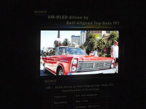
Sony developed a new OLED panel that uses a self-aligned top-gate Oxide-TFT (IGZO). According to Sony, the image is improved over normal OLEDs as it reduces the unevenness in brightness (that is caused by parasitic capacitance between gate electrode and source/drain electrodes in the TFT). The new panel is 9.9" in size (960x540) and features 200cd/m2 brightness, 1M:1 contrast ratio and 96% NTSC color gamut.
Sony's new TFT uses a self-aligned top-gate structure (Sony's older TFT used a bottom-gate structure). This makes it possible to keep a long enough distance between the gate electrode and the source/drain electrode - which reduces parasitic capacitance.
To make this new structure, Sony developed a new manufacturing process:
- Patterning with a dry-etching method after forming oxide semiconductor IGZO, gate insulating film and gate electrodes on a glass substrate
- Forming an aluminum thin film on it with a sputtering method
- Forming an aluminum oxide (Al2O3) protective layer by oxidizing Al in an oxygen annealing process and a low-resistance layer by dispersing enzyme on the surface of the oxide semiconductor (this adds stability and high reliability to the annealing treatment)
- Forming source/drain electrodes by opening via holes after forming an organic layer in a coating process.
Source:
Posted: May 24,2011 by Ron Mertens

