Fujifilm and imec have jointly developed a new photoresist-based OLED (and other organic semiconductors) patterning technology that can enable sub-micron patterns. The new process uses existing i-line photolithography equipment and may be a cost-effective production method for high resolution devices.
Photoresist technologies are based on photo-sensitive materials that cause photochemical reaction when exposed to light. This technology is already used for microfabrication in semiconductor production. The new process builds on Fujifilm's synthetic-organic chemistry material design technology.
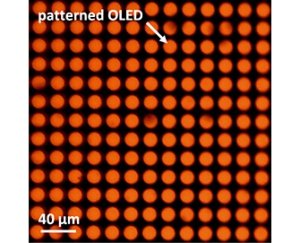
To test the new process, imec and Fujifilm developed two prototypes - an OLED and an organic photo detector (OPD) array. The OLED features 20 um pitch OLEDs (the diameter of these round pixels is 15 um) and it emits uniform light. The OPD elements are 200x200 um in size.
Fujifilm and imec plan to continue research and development to promote the industrialization of this technology. Fujifilm's entire OLED IP portfolio was bought by UDC in 2012 for $105 million, I did not know the company is still involved with new R&D in this area.

