Photolithography

TCL CSoT is deploying new OLED technologies at its production lines, including LTPO, micro lens and polarizer-free OLEDs

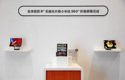
TCL (CSoT) announced that the company has finalized the development of several new OLED technologies, which has been deployed at the company's production lines.

TCL/CSoT 8'' PLP-LTPO foldable AMOLED prototypes (SID Displayweek 2022)

The first technology is LTPO, or Low-Temperature Polycrystalline Oxide, an OLED backplane technology developed originally by Apple. LTPO enables variable refresh rates, and TCL's technology can support a wide range of frequencies, from 1Hz to 144Hz.

Read the full story Posted: Jun 24,2022

The Holst Center to unveil new fingerprint sensor technologies at Display Week 2019

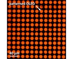
The Holst Centre announced that it will show several new fingerprint sensor innovations at Display Week 2019 next week. The research center will show a new high-resolution (500 PPI) under-the-display sensor that uses the Center's proprietary collimator technology as well as an in-display sensor concept that uses photolithography patterning to integrate the OLED and organic photo diodes (OPD) pixels side-by-side.

The Holst will also showcase a new over-the-display (suitable for LCDs) transparent sensor which at 70% the center says is the world's most transparent fingerprint sensor.

Read the full story Posted: May 11,2019

Researchers develop a sub-electrode micro-lens array that can increase the light output in OLEDs by a factor of 3

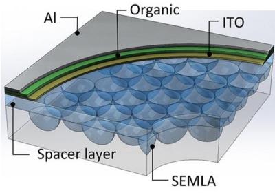
Researchers from the University of Michigan developed a new method to cost-effectively extra more light out of OLED displays. To achieve that, the researchers used a Sub-Electrode Micro-Lens Array (SEMLA) placed between the bottom transparent ITO electrode and the glass substrate. Testing on green and white PHOLEDs, the researchers say the SEMLA enhanced light output by a factor of 2.8 (green) and 3.1 (white) compared to a similar device without the lens array.

OLED micro-lens array (Michigan)

The researcher say that such an array can be fully transparent and has no impact on the sharpness of the display. The hexagonal array of 10 um lenses can be fabricated using conventional photolithography methods which are quite cost effective. Such a micro-lens array does not change the actual OLED production process.

Read the full story Posted: Apr 30,2018

CPT and imec demonstrate an 1250 PPI OLED patterned using a photolithography process

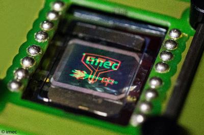
Taiwan-based Chunghwa Picture Tubes (CPT), in collaboration with European research institute imec (in the framework of the Holst Centre collaboration) have demonstrated an ultra-high resolution OLED display that was patterned using photolithography - without the need for an FMM (metal mask). A photolithography process offers a high aperture ratio, large substrate sizes and good yield control.

FMM-free photolithography-made OLED prototype (CPT + imec)

The prototype display that was demonstrated is a passive display with a 1400x1400 resolution (or 1250 PPI!) of side-by-side orange and green OLEDs. imec reports that preliminary lifetime investigation shows operation of each color after patterning for a few hundred hours at more than 50% of the original brightness.


Read the full story Posted: Sep 20,2017

Fujifilm and imec show a full-color photoresist OLED device prototype

Back in 2013, Fujifilm and imec jointly developed a new process to deposit and pattern OLED materials using existing i-line photolithography equipment. The two companies have now demonstrated a full-color photoresist OLED. They say that this could lead to a new process that can be used to produce high-resolution large-area OLED displays in a cost-effective way.

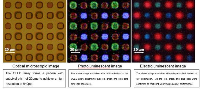
Fujifilm-imec full-color photoresist OLED (June 2015)

In the new prototype, the two companies patterned red, green and blue OLED materials to create a subpixel pitch of 20 micrometer. The full device is 40x40 pixels and achieved a density of 640 PPI. As you can see in the image above, UV rays were used to confirm the result.

Read the full story Posted: Jun 02,2015

Fraunhofer's Orthogonal Photolithography technology enables direct-emission OLED microdisplays

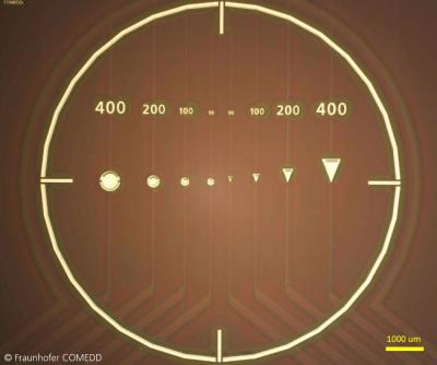
Fraunhofer COMEDD collaborated with Orthogonal Inc to develop a new approach for OLED micro-structuring. The new patented technology, called Orthogonal Photolithography allows direct patterning of organic material on CMOS-backplanes.

This technology can enable high-brightness (5000 cd/m2) high-resolution OLED microdisplays. This is because it can be used to create direct-emission OLED microdisplays. All current microdipslays on the market use white OLED subpixels with color filters. Fraunhofer is also developing direct-emission OLED microdisplays using flash-mask-transfer-lithography (FMTL) technology.

Read the full story Posted: Apr 24,2014

Fujifilm and imec developed new photoresist-based OLED patterning technology

Fujifilm and imec have jointly developed a new photoresist-based OLED (and other organic semiconductors) patterning technology that can enable sub-micron patterns. The new process uses existing i-line photolithography equipment and may be a cost-effective production method for high resolution devices.

Photoresist technologies are based on photo-sensitive materials that cause photochemical reaction when exposed to light. This technology is already used for microfabrication in semiconductor production. The new process builds on Fujifilm's synthetic-organic chemistry material design technology.

Read the full story Posted: Sep 29,2013

Companies show ITO-free, Printed Flexible OLED lighting, paving the way to low-cost large-size OLEDs

Agfa, Philips and the Holst Center are showing a large-area (12x12cm2) flexible OLED - without ITO as transparent electrode, and with printed shunting lines. This means that costly materials and lithography processes are not needed, and the OLEDs are much cheaper.

Flexible OLED lighting prototype with no ITO  photoFlexible OLED lighting prototype with no ITO

Up till now, ITO was needed as supporting layer for the PEDOT/PSS* anode layer with lower conductivity. Thanks to Agfa’s high-conductive transparent polymer OrgaconTM, a PEDOT/PSS-based solution with six orders better conductivity than its predecessor, the use of ITO can now be avoided. Proof is the latest OLED lighting demonstrator of Holst Centre’s shared programs: a homogeneous white OLED tile of 12x12cm2 without the use of ITO.

Read the full story Posted: Apr 07,2009

Georgia Tech and Solvay announce a $3 million OLED R&D deal

The Georgia Institute of Technology's Center for Organic Photonics and Electronics (COPE) and Solvay announced a $3 million deal for OLED research today.

Solvay, an international chemical and pharmaceutical group headquartered in Brussels, Belgium, with units in more than 50 countries and a strong presence in Georgia, has signed a three-year commitment with Georgia Tech to fund research in organic light-emitting diodes (OLEDs).

Read the full story Posted: Apr 26,2006