OLED is an emerging display and lighting technology that enables beautiful and efficient displays and lighting panels. Thin OLEDs are already being used in many mobile devices and TVs. Polymer-OLEDs (or PLEDs, also used to be called P-OLEDs) are OLED devices made from polymer (large-molecules) materials.

PLEDs vs SM-OLEDs
Basically you can make OLEDs from two kinds of materials: small-molecule (SM-OLED) or large-molecules, or polymers. Virtually all OLED displays on the market toady are using Small Molecules, and are produced using evaporation processes.
PLED (P-OLED) materials do not perform as good as SM-OLEDs in terms of lifetime and efficiency, but are easily soluble and so can be easily adapted for printing and other solution-based processes. In the past some believed that the soluble nature of PLEDs mean that these materials will be the future of OLED displays, but that has not been the case yet. There has been great progress in evaporation processes and materials - and also in soluble SM-OLEDs.
CDT / Sumitomo
UK-based Cambridge Display Technology (CDT) is the company that holds the basic patents for PLED technologies. The company licensed its technology to several companies, including Philips, Seiko Epson, Osram, Dupont and Delta Optoelectronics, but it does not seem as it anyone is pursuing PLEDs at the moment besides Sumitomo Chemicals (which owns CDT).
Sumitomo and CDT are still developing PLED materials and panels. Sumitomo is providing emitter materials for JOLED (who started low volume production of printed OLED monitor panels in December 2017, see below) and is hopefully gearing up to start mass production of its own OLED lighting panels.
JOLED's PLED
JOLED (Japan OLED) was established in August 2014 by Japan Display, Sony and Panasonic with an aim to become an OLED medium display (10-30 inch) producer, mostly targeting monitors and commercial applications. JOLED is using a printing process which should result in lower cost production (but of lower performance displays) compared to evaporation printing.

JOLED is using PLED materials produced by Sumitomo (see above). The company started commercial low-volume production of its 21.6" 4K OLED panels towards the end of 2017 at the company's pilot 4.5-Gen line. In 2021 JOLED started mass producing PLED displays at its 5.5-Gen line in Nomi City.
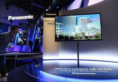
Panasonic's 2013 56" OLED TV prototypes
In January 2013 Panasonic unveiled a 56" 4K (3840x2160) OLED TV panel prototype that was produced using an all-printing method and PLED materials. Panasonic says that all the organic materials were deposited using ink-jet printing. The panel's TFT substrate was supplied by Sony (and actually made by AUO. It's an Oxide-TFT panel) as part of the two companies collaboration. The lifetime and efficiency of this TV was not disclosed.
In December 2013 Sony and Panasonic announced that they are canceling the OLED TV JV. Panasonic is now producing OLED TVs - but these use WRGB OLED panels produced by LG Display.
P-OLED (PLED) vs pOLED
P-OLEDs, or PLEDs, are a class of OLED materials. Somewhat confusingly, LG Display is branding its mobile flexible AMOLED displays as pOLEDs (plastic OLEDs). For more information on LGD's pOLEDs, click here.
Further reading
The latest PLED news:
Digitimes: Japan earthquake did not have a serious impact on OLED companies (updated)
Update: Digitimes posted a full list of earthqake effects on Japanese OLED plants and facilities.
According to Digitimes, the Japanese earthquake did not have a serious impact on OLED companies. The only company that was really hit was Showa Denko - and while it's not clear from the article is seems that the damage is not substantial. Sumitomo's PLED production saw some 'modest' disruption as well.
Idemitsu Kosan was only effected by the transportaion and power outrages. It's not clear how did TDK (who makes PMOLED panels) fare.


New low-cost OLED lighting project gets funding from the UK
A new project called TOPDRAWER (Thin organic prototypes, design, research, applications with end-user recognition) has secured funding from the UK government, and will start in early November and will run for 2.5 years. This is actually a followup project to TOPLESS, and is also lead by Thorn lighting.
 TOPLESS project OLED lamp prototype
The consortium will develop and demonstrate a printed manufacturing process that will be integrated into attractive designs that have been created through consultation with potential end-users. The manufacturing process will be proved and tested within PETEC, that will acquire and install a large-area coating line.
Sumitomo Chemical developed a new 6.5" OLED panel
Sumitomo Chemical has developed a new 6.5" AMOLED panel. It's a polymer-based OLED made by printing technology, sealed by a metal plate. It was made by Sumitomo's "Device Development Center," which was established in August 2009.

Updates from Merck's OLED VP - focusing on solution-processable OLED materials
![]()
 In February 2009, we interviewed Dr. Udo Heider, Merck's OLED Unit VP. Merck is a global pharmaceutical and chemical company based in Germany, working on high performance OLED materials. Dr. Heider was kind enough to do a follow-up interview with us...
Q: Dr. Heider, thanks for taking the time to do this second interview... Back in February you said that within nine months you'll have a solution-processable Green OLED ready. Any updates on that? What about Blue and Red?
Indeed it is with great pleasure for me to report that our development team has really done an excellent job in making progress and delivering results in the area of solution-processed OLED materials. Merck can now report that in a spin coating process, the gap between solution and evaporation processed phosphorescent green materials has been almost completely bridged. Merck is now shifting its focus to the implementation phase: this means working together with world renowned process and display manufacturers to make sure that these materials can now be printed in line with performance and yield requirements. We hope to report on results in this area in the near future. The extensive know-how that has been accumulated during the last couple of months in the areas of Green can now be transferred with confidence to the other primary colors Red and Blue. The key to success is based on combining the learnings and strengths of the Small molecule and Polymer OLED worlds.
CDT and CIT Demonstrate ITO-Free PLED Lighting Panel
![]() CDT say they have produced an ITO-free PLED Lighting device, using a fine copper mesh. They have collaborated with Conductive Inkjet Technology (CIT) in the NOMAD project funded by the UK's government.
CDT say they have produced an ITO-free PLED Lighting device, using a fine copper mesh. They have collaborated with Conductive Inkjet Technology (CIT) in the NOMAD project funded by the UK's government.
ITO is expensive and brittle, and is not so useful for flexible electronics. The new manufacturing method demonstrated in the NOMAD project reduces costs by eliminating ITO along with significantly reducing the capital and processing costs for patterning metal bus bars which distribute current and ensure the uniformity of light emission. CIT’s process eliminates the need for traditional vacuum sputtering equipment and etching tanks.
Interview with David Fyfe, CDT's Chairman and CEO
![]() CDT is one of the leaders in OLED research, focusing on Polymer-based OLEDs (PLEDs, also called P-OLEDs). While these OLEDs are lagging behind small-molecule OLEDs in current products (all AMOLEDs today are based on SM-OLEDs), some companies believe that PLEDs are actually the better tech for the future.
CDT is one of the leaders in OLED research, focusing on Polymer-based OLEDs (PLEDs, also called P-OLEDs). While these OLEDs are lagging behind small-molecule OLEDs in current products (all AMOLEDs today are based on SM-OLEDs), some companies believe that PLEDs are actually the better tech for the future.
CDT's CEO, David Fyfe has agreed to answer a few questions we had on CDT's technology. David joined CDT in 2000 as Chairman and CEO. David saw CDT go public in 2004, and then negotiated the sale of CDT to Sumitomo for $285 million (in September 2007). David is also a director of Soligie, an electronics printing company, Acal Energy, a fuel cell technology developer and the Plastic Electronics Foundation.
Q: David - thanks for agreeing to do this interview. Since the Sumitomo acquisition, CDT has been rather quiet... can you give us an update on where's the company now, and where's it is headed?
Since the merger of CDT into Sumitomo Chemical in September 2007, CDT has grown substantially and received considerable capital investment to enable it to remain a leading developer of PLED technology. It works very closely with SCC laboratories in Japan and most recently has been transferring manufacturing process knowhow to SCC's own PLED manufacturing development line, recently commissioned at Ehime on Shikoku, Japan. CDT in partnership with SCC has made large strides in materials lifetimes and efficiencies. SCC prefers to take a lower profile in announcing these advances since its business model is to work with selected display maker partners in a collaborative, confidential relationship. We have also made big strides in the development of top emitting structures and in printing PLED displays. SCC's strategy is that CDT will continue to be its leading development center for PLED technology with Ehime scaling process technology to a yielding process status. CDT is also working very closely with Semprius of North Carolina, USA to develop single crystal silicon TFT structures on which PLED devices can be deposited and driven using Semprius’ proprietary stamping technology.
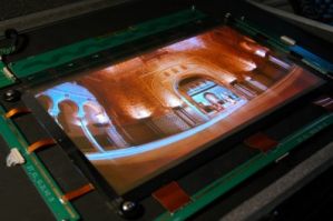 CDT 14-inch OLED prototype from 2005
Q: It seems that OLED displays are finally entering the mainstream - we hear of new devices (mainly by Samsung, but also from Sony, Microsoft, LG and others) almost daily. What are your thoughts on this? what are the challenges that still exist for OLEDs?
Sony broke the logjam of resistance to the adoption of OLED in large displays by major display makers with the introduction of its XEL-1 11 OLED TV in 2007. Samsung SDI’s investment in small screen OLED production in 2007, based on LTPS backplanes was another major impetus. Since then, Chi Mei has brought on small OLED screen capacity, TMD (now wholly owned by Toshiba) has built an OLED line to manufacture small screens, LG Display will start up their Gen 3.5 line late this year and if press reports are to be believed, Toppoly will commission their capacity with Nokia as a lead customer and Panasonic have a major OLED development program for large OLED displays.
Seiko Epson sees 37" (and larger) inkjet-printed OLED TVs in 2012
Last month Seiko Epson has unveiled a new inkjet-printing technology for OLEDs, suitable for large sized panels. We have talked to Satoru Miyashita, General Manager of Seiko Epson's Core Technology Development Center about this new technology and their plans for OLED production.
Q: You have shown a new ink-jet based OLED technology. You say it will enable 37" or larger HD-OLED TVs. Do you have any plans to actually make such TVs? When do you think products can be made with this new tech?
Epson is currently considering a variety of options regarding the commercialization of this technology, but at this point no specific announcements have been made about plans. We see 2012 as being the year that 37"+ OLED TVs will be launched by various makers, and 2015 as the year that sales will really take off for this market.
 Espon 14-inch Inkjet processed OLED
Panasonic teams up with Sumitomo for OLED TVs
Panasonic has announced that they are developing OLEDs together with Sumitomo. They aim to make 40" (or bigger) TVs by 2010. Back in 2008, Sumitomo announced plans for OLED TVs by 2009, and were seeking partners for doing it.
Sumitomo's technology is based on CDT's PLED materials (CDT were acquired by Sumitomo back in 2007).
Plextronics Says Their Printable Ink Improves Performance in PLEDs
![]() Plextronics announced today that its conductive ink has been shown to improve the performance of certain PLED devices.
Plextronics announced today that its conductive ink has been shown to improve the performance of certain PLED devices.
CDT will use new Printing technology to improve OLED performance
 Cambridge Display Technology (CDT) will develop a new technology to make OLED backplanes, together with Semprius. The new tech will be integrated into CDT's 14-inch development line at Godmanchester campus, near Cambridge, UK.
Semprius has a technology for semiconductor printing, and the two companies will use the technology in the manufacturing of OLED backplanes.