Nanomarkets: solution-processed OLED materials to take up 47% of the OLED market by 2019

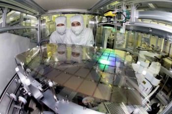
Nanomarkets released a new white paper about solution-Processed OLEDs. They estimate that in order for the OLED market to grow significantly for TV and lighting applications, companies must adopt solution-processable materials. Soluble OLEDs have been researched for years with very little outcome outside of the lab. But Nanomarkets believes that the current problems can be fixed, and are worth fixing.

Soluble OLED materials and appropriate processes are being researched by Sumitomo, DuPont, Pioneer, UDC, Solvay, Marck and others. They estimate that the first panels to be made using these materials will be Pioneer's (together with Mitsubishi) OLED lighting panels - planned for 2014. Nanomarkets thinks that if Pioneer succeeded, it may push GE back into the OLED game with their own soluble material solutions. It's interesting that Nanomarkets does not mention Panasonic's OLED TV prototype that uses Sumitomo's P-OLED materials.

Read the full story Posted: Apr 04,2013

AUO is looking into an OLED printing process

Digitimes reports that AUO has started to develop a printing process to make OLED panels, with hopes that this new process will lower the production cost and increase the material utilization. AUO is suffering from low (50%) yields in its current production process - which uses vapor deposition. The report suggests that AUO is also developing Oxide-TFT backplanes for OLEDs - but this isn't news - AUO unveiled an Oxide-TFT based 32" OLED TV prototype back in November 2011.

AUO 32-inch AMOLED prototype

Actually all OLED makers are looking into more efficient production processes based on printing so this is hardly a surprise. It's likely that it will take some years before we'll start seeing printed OLED panels on the market though.

Read the full story Posted: Sep 27,2012

Panasonic re-organizes to put more focus on OLED displays

According to a report from Nihon Keizai, Panasonic has taken steps to streamline its R&D and put more focus on OLED TV development. The company plans to invest ¥30 billion ($385 million) in a pilot AMOLED production line in Himeji (this was already reported in April). According to the report Panasonic wants to use PLEDs and ink-jet printing in its upcoming fab. Panasonic's P-OLED/Ink-jet development dates back to the OLED TV joint-venture with Sumitomo in 2009.

Sony OLED TV prototypeSony OLED TV prototype

The report also details the collaboration between Panasonic and Sony. The two companies have quite different technologies - Panasonic with its P-OLED and printing processes and Sony with small-molecules and VTE. It is claimed that Sony will mostly supply capital for Panasonic, and not technology. Sony's own OLED technology will be used though by Japan Display to make small sized panels.

Read the full story Posted: Sep 12,2012

LG Display suspected of OLED technology theft from Samsung Mobile Display

Last month we reported that the Korean police is investigating a case of AMOLED technology leaking from Samsung Mobile Display to a "local rival firm". We suspected the rival firm is LG Display, and today this is confirmed. The Korean police announced that they are questioning 10 LG Display employees, all former SMD employees. LGD's stock fell around 5% on the news.

This technology is Samsung's Small Mask Scanning, used to produce AMOLED on large substrates.


Read the full story Posted: May 03,2012

OFT Edge - a new OLED deposition system by VG Scienta

VG Scienta announced a new OLED deposition system, the OFT EDGE. The OFT (Organic Flexible Transparent) system can be used to deposit and analyse organic and inorganic layers on flexible and solid substrate.

The OFT Edge technology provides low temperature deposition of TCO, metals, small molecule deposition for organics, and an interchangeable modular construction with a wide selection of both deposition and analytical tools that can be attached to the systems to further increase the flexibility of the tool. VG Scienta offers ALD modules, XPS/UPS modules, STM, IR, and AFM modules. Modules within the system can be used as either standalone units when combined with a fast entry load lock or can be fully integrated into the multi-purpose cluster tool in conjunction with a central handler.

Read the full story Posted: Feb 16,2012

AUO - we'll unveil OLED TV samples by end of 2012

AU Optronics announced their financial results for 4Q 2011, with a record loss of $21 NT billion (almost $700 million USD). AUO is hoping to return to profitability - mostly because of growth in demand for LCD TVs in emerging markets such as India, Indonesia and Brazil. Regarding AUO's OLED program, the company re-iterated plans to mass produce AMOLED panels for mobile phone in this quarter (a little sooner then expected, actually), and more interestingly they said they plan to unveil OLED TV panel samples by the end of 2012.

AUO 32-inch OLED TV prototype

AUO already unveiled a 32" OLED TV prototype back in November 2011, but they probably want to unveil larger panels towards the end of the year - and ones that are closer to mass production. The 32" prototype AUO shows had a Oxide-TFT (IGZO) backplane and was fabricated using vapor deposition using a metal mask. The panel featured Full-HD (1920x1080) resolution, 100,000:1 contrast ration, 0.01ms response time and brightness of 200cd/m2.

Read the full story Posted: Feb 09,2012

Jusung developed a MOCVD IGZO TFT Process

Jusung Engineering reports that they managed to developed a a new metal organic chemical vapor deposition (MOCVD) technology to apply IGZO for use on flat panels. Jusung says they are the only company to develop an 8-Gen MOCVD IGZO tool, and that this technology will be compatible with future OLED display processes. We talked to Jusung and they say that they are already in talks with several potential clients (in Japan, China and Korea) and they hope to get purchase orders and start shipping equipment in the middle of 2012.

There are other methods (such as sputtering) for IGZO production. Sharp will soon start to produce IGZO displays in their upcoming production line, and over the past year we've seen IGZO OLED prototypes by Sony, Toshiba, AUO and other companies. Most (or all) of these prototypes have been developed using sputtering. Jusung claims that MOCVD will enable higher resolution than sputtering - indeed 4 or even 5 times higher! They also say that scaling sputtering to 8-Gen will be difficult, while their own MOCVD tool will be scalable up to these sizes easily.

Read the full story Posted: Nov 27,2011

The Flexible Display Center installed a new Gen II OLED process tool

The Flexible Display Center (FDC) at Arizona State University (ASU) installed Sunic Systems' GEN-II OLED SUNICEL Plus 400 vacuum evaporation and encapsulation process tool. The FDC now has the ability to manufacture full color flexible OLEDs in-house - and the FDC says that they are already scaling the recently announced 3.8" AMOLED prototype (developed together with Universal Display, shown below) to larger sizes. The FDC purchased that system back in May 2010.

The FDC says that this new Gen II production system will enable the development of not only large-size flexible OLEDs but also solid-state lighting and plastic electronics.

Read the full story Posted: Jun 29,2011