Futaba developed a new thin PMOLED panel, will start production towards the end of 2012

Futaba says they have developed a new thin PMOLED display - in fact it's one seventh as thin as their existing PMOLEDs at 0.29 mm (Futaba's regular PMOLEDs are 2 mm thick). The new display is also much lighter: a 2.7" panel weights 1.3 grams. In order to make these new displays Futaba developed new materials and eliminated the hollow structure used to protect the OLED materials.

Futaba will begin mass producing the new displays towards the end of 2012. The new displays will cost about 50% more than Futaba's thicker panels.

Read the full story Posted: Jun 17,2012

Sony explains the technology behind their OLED microdisplays

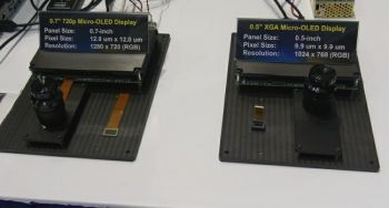
Sony released 0.5" 1024x768 (2,560 ppi, 9.9um pixel pitch) and 0.7" 1280x720 (2,098 ppi, 12um pixel pitch) OLED microdisplays back in August 2011, and now they gave some interesting details about the technology used to fabricate those panels. The 0.5" OLEDs are used in several 'A' class digital cameras, and the 0.7" microdisplays are used in the HMZ-T1 HMD device.

We already know that the microdisplays use white OLEDs with RGB color filters (all OLED microdisplays on the market use this architecture, although eMagin are working on direct-emission ones). Sony are using stacked RGB fluorescent materials. They say they did not choose red and green PHOLEDs because of lifetime, reliability and cost considerations.

Read the full story Posted: Jun 17,2012

Quantum Dots at SID: 3M to commercialize QDEF, Some QD Vision updates

I visited two companies active with Quantum Dots for displays at SID. First up was Nanosys, which developed their quantum dot enhancement film (QDEF) technology - which dramatically improves LCD color. Nanosys showed a couple of comparisons at their booth of Apple's iPad 2 and an LCD TV - with and without the QDEF film.


The comparison was quite good, and the displays that feature the QDEF films had more vibrant colors. However, compared to Samsung's and LG's OLED TVs, those LCDs were still bland to my taste. But maybe I'm not really being objective here.

Read the full story Posted: Jun 17,2012

Ignis Innovation at SID 2012

As I already said before, Ignis Innovation's SID booth was one of the conference highlights for me. Their technology is very impressive and hopefully will enable cheaper non-LTPS AMOLED production.


In their booth, Ignis were showing 3.5" and 20" AMOLED panels that use the company's a-Si backplane compensation technology. The panels were made by RiTdisplay. Ignis and RiTdisplay have been showing these displays back in 2011. Originally they were supposed to be released towards the end of 2011, but this never happened. During SID Ignis announced that now the plan is to release these by the end of 2012. According to Ignis the 3.5" AMOLED will be cheaper than the LTPS-based competition (i.e. Samsung made panels). You can read more about these panels and RiTdisplay's plans at my RiTdisplay-at-SID-2012 post.

Read the full story Posted: Jun 16,2012

RiTdisplay at SID 2012

RiTdisplay is a PMOLED producer based in Taiwan that has several production lines making PMOLED panels. A few years ago it was considered the world's largest PMOLED maker, although I now hear that due to financial problems the company shut down some of their PMOLED lines (this isn't confirmed though).


At SID 2012, RiTdisplay showed several PMOLED panels, and some 3.5" AMOLED panels. RiTdisplay is Ignis' production partner for its a-Si compensation technology, which basically enables a-Si to be used as a backplane for AMOLED panels (instead of LTPS or Oxide-TFT). This should enable cheaper AMOLEDs. You can read more about this technology at my Ignis-at-SID post.

Read the full story Posted: Jun 16,2012

eMagin at SID 2012

One of the first companies I wanted to visit at SID was eMagin. I met the company's CEO (Andrew G. Sculley) for the first time, and he gave me a very nice introduction to the company's current business and future plans. I'll try and summarize that meeting and eMagin's booth in this post.


eMagin is now in the final testing and qualification stages of its new deposition and seal machines. Those new machines are expected to increase capacity and improve yields. It will also free up the current machines for R&D, which seems to be very important for Andrew.

Read the full story Posted: Jun 16,2012

Samsung's Galaxy SIII now shipping from AT&T for $189.99

According to Amazon, the Galaxy S3 is now shipping for AT&T for $189.99 (including a contract of course). I think that's the first carrier to actually ship this phone in the US. The Galaxy S3 US model has a 4.8" 1280x720 HD Super AMOLED (with Pentile), a dual-core 1.5Ghz CPU, 2GB of RAM and an 8 mp camera (1080p video) and lot's of new software features. The phone weighs 133 grams and is only 8.6 mm thick.

The S3 pre-order numbers were very strong, and it seems that Samsung has another winner at their hands, we'll be sure to hear from Samsung about actual sales numbers soon.

Read the full story Posted: Jun 16,2012

LG Display at SID 2012

LG Display had a very big booth at SID 2012, showing lot's of displays. The main item on show was the 55" OLED TV panel, but all the rest of the displays were LCDs. As I said in my first post from SID, LG's OLED TVs stunning with great colors, amazing contrast and excellent 3D effects. Unlike Samsung, LGD had only one TV on show, showing 2D and 3D convent sequentially (the 3D uses passive glasses). LG's OLED panel is extremely thin - 4 mm, you can hardly see it looking from the side.


During LG Display's keynote speech, they made some very interesting comments about their OLED technology and business. First of all, LG expects OLED TVs to grow at 320% (CAGR) from 2012 to 2016, reaching 11% of the TV market, while the rest of the market - LCD/PDP/CRT will only grow at 1.1%. OLED TV is the "next evolution" of TV technology.

Read the full story Posted: Jun 16,2012

Sony believes its offset printing technology could enable 500ppi OLED panels

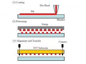
At SID 2012 Sony presented a technical paper describing its offset printing technology which enables high resolution OLED panels. In fact Sony claims this technology could produce 500ppi OLED panels.

Sony's printing technology has three steps. In step 1, the ink is coated on a flat blanket by slit coating. In step 2, the stamp and the blanket are then placed in contact and subsequently separated. The ink in contact with the stamp detaches from the blanket, since the stamp has a higher surface energy than the blanket. The stamp has the reverse pattern. As a result, the desired print pattern remains on the blanket.

Read the full story Posted: Jun 16,2012

Plastic Logic to develop plastic amorphous polymers and OTFTs for OLED displays

The UK's Technology Strategy Board (TSB) is funding 43 new projects under the ‘Technology Inspired Innovation’ R&D competition. Plastic Logic will participate in two of these projects, both related to OLEDs. The first one aims to develop new high-performance amorphous polymers, and the second called ROBOLED aims to integrate organic thin-film transistors (TFTs) backplanes with OLED frontplanes. Plastic Logic is collaborating with the UK's CPI on this project.


Back in January 2011 Plastic Logic received $700 million in funding from Russia's RusNano fund - to build a mass-production factory for thin, light and flexible plastic-based e-paper displays. The company recently withdrew from the e-reader market, and is now focused on technology licensing.

Read the full story Posted: Jun 15,2012