At SID 2012 Sony presented a technical paper describing its offset printing technology which enables high resolution OLED panels. In fact Sony claims this technology could produce 500ppi OLED panels.
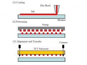
Sony's printing technology has three steps. In step 1, the ink is coated on a flat blanket by slit coating. In step 2, the stamp and the blanket are then placed in contact and subsequently separated. The ink in contact with the stamp detaches from the blanket, since the stamp has a higher surface energy than the blanket. The stamp has the reverse pattern. As a result, the desired print pattern remains on the blanket.
In the final step, the TFT substrate and the blanket are aligned, placed in contact and finally separated. The print pattern is transferred from the blanket to the TFT substrate based on the same principle as that for the second process.

Sony has developed a printing system based on this technology for a Gen-1 (300x350 mm) substrate, and already produced 3" VGA panels (270 ppi). If I understand it correctly, this is the panel Sony unveiled last year on May 2011 at SID, shown above.