Ths is a guest post by Ajit Krishnan, Director, New Business Development, Office of the CTO, Applied Materials, Max McDaniel, VP/CMO Display Business Unit, Applied Materials, Gunther Haas, CTO MICROOLED, and Thierry Bissuel, CEO MICROOLED.
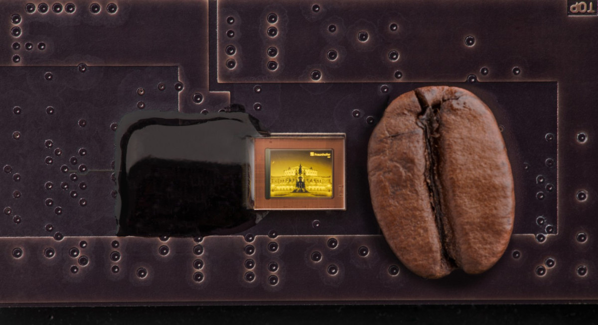
The pursuit of the ideal AR/VR microdisplay has become one of the most complex engineering challenges in our industry, with massive investments and the trajectory of spatial computing at stake. At its core lies a deceptively simple problem: how to produce red, green, and blue light from pixels 50 times smaller than a strand of human hair—without compromising efficiency, color accuracy, or the ability to manufacture at scale for mass adoption.
While many in the industry continue to wrestle with this challenge, evidence suggests that Si2OLED technology provides a compelling solution. To appreciate the significance of this approach, it is important to examine the prevailing methods in the market—and understand where they fall short.
Today’s leading commercial OLEDoS microdisplays largely rely on a white OLED combined with color filters (W-OLED + CF). In this setup, a white light source illuminates all pixels, and filters selectively pass red, green, or blue light to form images. This is the same architecture used in displays from companies like Sony, including those found in devices such as Apple Vision Pro. While functional, this design suffers from a fundamental limitation: color filters inherently waste light. Only about 25% of the emitted light contributes to the final image, while the rest is absorbed. This inefficiency forces higher driving currents to achieve acceptable brightness, increasing power consumption, accelerating material degradation, and ultimately reducing device lifespan. In addition, in order to reach the required brightness levels, WOLED+CF architectures require the use of stacked, so-called tandem OLED devices which require a high operating voltage of around 12V which puts severe constraints on the CMOS backplane technology.