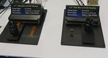
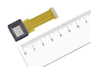
Sony released 0.5" 1024x768 (2,560 ppi, 9.9um pixel pitch) and 0.7" 1280x720 (2,098 ppi, 12um pixel pitch) OLED microdisplays back in August 2011, and now they gave some interesting details about the technology used to fabricate those panels. The 0.5" OLEDs are used in several 'A' class digital cameras, and the 0.7" microdisplays are used in the HMZ-T1 HMD device.
We already know that the microdisplays use white OLEDs with RGB color filters (all OLED microdisplays on the market use this architecture, although eMagin are working on direct-emission ones). Sony are using stacked RGB fluorescent materials. They say they did not choose red and green PHOLEDs because of lifetime, reliability and cost considerations.
Sony says that the ETL, EML and HIL/HTL layers were optimized for improving the light-emitting materials' quantum efficiency and stabilizing the balance of their carriers. The blue element for example uses an ETL of 140nm, an EML of 30nm and HIL/HTL of 40 nm - which realizes a high quantum efficiency and a long product life at the same time.

