Toshiba, Panasonic and the FDC developed new flexible OLED panels

Several companies announced new flexible OLED panels at SID 2013. None of the panels were demonstrated (except for Toshiba which showed the OLED but it was not powered). First up is Toshiba, which showed a 10.2" 1920x1200 (223 PPI) panel. Toshiba's OLED has an Oxide TFT backplane and uses the WRGB (white OLED with color filters) architecture.

Toshiba flexible OLED prototypeToshiba flexible OLED prototype

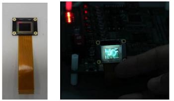
Panasonic developed a 4" flexible OLED with 224x224 resolution (only 80 PPI, direct emission). Panasonic used PEN as a substrate and the panel can be bent up to a curvature radius of 10 mm. This is also an Oxide-TFT panel. To produce it, Panasonic attached the PEN sheet to a glass substrate, deposited the OLED materials and then de-laminated the glass.

Read the full story Posted: May 26,2013

Nanomarkets sees a $4.6 billion OLED materials market in 2020

Nanomarkets published a new edition of their OLED Material Market report, and they have some interesting forecasts and insights. Basically the company is upbeat on OLED displays for mobile devices, and the OLED TV market as well. While they are still cautiously optimistic that the long-term prospects for OLED lighting, they say that it will take many more years for this to become a major outlet for OLED materials.

Nanomarkets projects that the total market for OLED materials will grow from about $450 million in 2013 to over $4.6 billion by the end of 2020 - mostly from mobile displays and OLED TVs. Core OLED materials (emitters, hosts, dopants, HIL, HTL, etc. but excluding substrates, encapsulation, electrodes, etc.) will grow from $265 million in 2013 to over $1.6 billion by 2020.

Read the full story Posted: May 26,2013

Ignis launched a new all-electrical inspection system for AMOLED production lines

Ignis innovation announced a new all-electrical inspection system for AMOLED manufacturing lines called MaxLife Inspection. This system provides information on each individual pixel and detects defects which can be repaired using a laser system. This system will increase yields by 2-5 times according to Ignis.

The MaxLife Inspection system uses a probe card, custom electronics and the MaxLife Viewer software to measure the brightness of every pixel in an OLED display with a 14-bit resolution. The system can be used before OLED deposition on the TFT backplane to find defective pixels and explain why they failed (this can be fixed by laser or new a deposition pass). The system can also be used after the OLED deposition to detect OLED defects (shorted pixels, etc.). It can also detect uniformity problems (such as speckles, "Mura" issues, etc.) after the final assembly of the panel.

Read the full story Posted: May 26,2013

LG Chem's publishes two nice OLED lighting videos

LG Chem published two nice (and short) videos showcasing their OLED Lighting panels. The first video introduces their 100x100 mm and 50x20 mm panels (with 45 or 60 lm/w). It shows several lumiaries from WAC Lighting, Acuity Brands and others.

The second video shows LG Chem's booth at EuroLuce 2013. Here you can see two LG Chem designed lamps that use their upcoming flexible OLED lighting panels (50x200 mm):

Read the full story Posted: May 26,2013

Panasonic developed a 114 lm/W OLED panel - claims world's most efficient panel

Panasonic Corporation developed a white OLED lighting panel that is the world's highest luminous efficiency - 114 lm/W for a light-emitting area of 1 cm2. Panasonic also developed a larger panel (25 cm2) with 110 lm/W. The panels also feature long lifetime - over 100,000 hours (LT50) and a brightness of of 1,000 cd/m2. The panel thickness was less than 2 mm.

Panasonic 114 lm/W OLED panelPanasonic 114 lm/W OLED panel

To achieve this high efficiency, Panasonic focused on an all-phosphorescent design (with an optimal stacked layer design) and new light extraction technology. Panasonic used a Built-up Light Extraction Substrate (BLES) by optimizing the arrangement of the film, glass and air to suppress light confinement in the OLED. This enable them to achieve about 2.5 times improvement in the light extraction efficiency, which is about 50% in the new panels. Panasonic says that in older technology the light extraction efficiency stayed below 40%. Panasonic says they hold 30 patents in Japan and 17 overseas - all related for this new development.

Read the full story Posted: May 25,2013

Philips installs a LivingScrulpture 3D OLED system in their New Jersey office

Philips just sent us a note saying that they installed a LivingScrulpture 3D OLED system in their Somerset (New Jersey) office's lunch area. The LivingScrulpture 3D is a kinetic system based on modular OLED blocks.

The system in Somerset uses 36 base modules for a total of 576 OLED panels. Each OLED panel is 76x76 mm in size (active area 61.4x60.5 mm) and the color temperature is 3,000K. The price of each base module is about â‚¬1500 - which means that this system costs about â‚¬55,000.

Read the full story Posted: May 25,2013

Samsung Display did develop an OLED microdisplay, back in 2011

Two days ago we reported on rumors that Google's next gen Google Glass HMD (or "wearable computer") will use OLED microdisplays made by Samsung Display. I wrote that as far as I know SDC never developed OLED microdisplays, but apparently I was wrong.

One of my sources sent me a conference paper from 2011 describing a 0.6" XGA OLED microdisplay - made by Samsung Mobile Display. The OLED-on-silicon device (Samsung calls them OLEDoS) used white OLEDs with color filters (all OLED displays made today use this architecture, although makers are moving towards direct emission). I don't think Samsung ever produced such displays, but apparently they did make some successful prototypes.

Read the full story Posted: May 25,2013

Samsung established new US patent firm, buys display patents (probably OLED) from Seiko Epson

Samsung Display Corporation (SDC) established a new company to handle patent trading and development in the US. The new company is called Intellectual Keystone Technology (IKT) and it was established in Delaware in March 2013.

Reportedly Samsung invested $25 million in the new company. On April 30 IKT bought several patents from Seiko Epson. According to reports, these are LCD and OLED related patents.

Read the full story Posted: May 25,2013

Samsung shipped over 10 million GS4 phones in less than a month

Last week Samsung reported that they will soon reach 10 million Galaxy S4 sales, and yesterday (May 23) they announced that indeed they surpassed that number. It took samsung less than a month to do so. The company hopes to sell over 100 million GS4 units - or double the GS3 sales. The GS4 is currently available in more than 110 countries and will be rolled out to a total of 155 countries soon.

The GS4 features a 4.99" Full-HD (1920x1280, 441 PPI) Super AMOLED display, an Octacore 1.6Ghz Exynos CPU (some models use a Quadcore 1.9 Ghz Qualcomm CPU), 2GB of memory, 13 mp camera and a 2,600mAh battery - all this while being a smaller and lighter than the GS3. The GS4 includes a lot of new software features and special UI controls, include the Adapt Display which allows extensive display calibration adjustments.

Read the full story Posted: May 24,2013

3M are in the final stages of scale up for LCD QDEF quantum dots films

Back in May 2012, 3M teamed up with Nanosys to commercialize QDEF Quantum Dot films for LCD displays. Today 3M announced that it is in the "final stages of scale-up" for these QDEF films. They plan to offer these to LCD makers that can be use them to make phones, tablets and TVs lighter, brighter, more energy efficient and with a larger color gamut. 

In January 2013 Sony unveiled some new LED-backlit LCD TVs under the Triluminos brand, which use QDvision's quantum dot films. This TVs (and smaller sized LCDs in one of Sony's digital cameras) are already shipping.

Read the full story Posted: May 24,2013