PECVD

UBI Research sees PECVD as the in-organic TFE equipment of choice for flexible OLED production

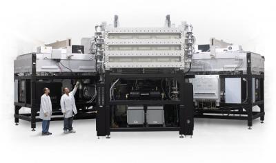
UBI Research says that as OLED makers are diverting all efforts into flexible OLED production, thin film encapsulation (TFE) is gaining in popularity. Between 2017 and 2021, TFE will be applied to about 70% of all OLED panels in production. The OLED encapsulation equipment market will generate $11 billion in sales.

PECVD oled encapsulation market share (UBI, 2017-2021)

TFE encapsulation started out as a complex technology that required 11 layers and was slow and expensive. Recent advances allowed OLED makers to reduce the number of layers to just 3 and increase productivity and yields and so lower the production costs. Some film OLED makers opted for hybrid encapsulation (which uses a barrier film) but TFE seems to have become the technology of choice.

Read the full story Posted: Jul 29,2017

Solmates sold a PLD tool for ITO deposition to CSOT's R&D line in Wuhan

Production laser deposition equipment developer Solmates announced that it has sold a small panel (200x200 mm) PLD tool to CSOT, to be used in the company's pilot OLED line that is being built in Wuhan, China. CSOT will use the new tool to deposit the ITO electrodes on OLED displays.

Solmates patented the process of OLED ITO electrode deposition using PLD and has developed the technology that enables large-area deposition of ITO on room temperatures. The PLD process results in very high quality ITO deposition and Solmates says that the achieved transparency is higher than currently used methods. Solmates' tool will be placed in CSOT's new cluster tool that is place in Wuhan since the end of 2016. Solmates will deliver the tool in June 2017. The current tool is used for R&D, but the technology can be scaled to larger substrates and to be used in production systems.

Read the full story Posted: May 25,2017

Meyer Burger ships an inkjet+PECVD OLED encapsulation system to an Asian customer

Meyer Burger announced that it has shipped a CONx TFE OLED thin film encapsulation system to an Asian customer. This system includes two deposition technologies, inkjet printing and PECVD to offer a complete encapsulation solution for flexible OLEDS.

Meyer Burger CONx TFE system photo

The CONx TFE system compreses of Meyer Burger's proprietary remote plasma PECVD for inorganic coating and its PiXDRO inkjet printing technology for the deposition of accurately positioned and homogeneous organic layers. Meyer Burger says that the system provides excellent water and oxygen barrier properties without compromising the optical transparency of the encapsulation layer all the while operating at low temperatures and low ion bombardment.

Read the full story Posted: Jan 06,2017

Both Samsung and LG to switch to ALD for in-organic TFE?

A few days ago we reported that Kateeva says it has taken a "commanding lead" in the OLED thin film encapsulation (TFE) market with its ink-jet based systems. Kateeva's ink-jet printers are used to deposit organic materials, but the full TFE stack also contains in-organic materials.

Currently both LG and Samsung producers are using PECVD to deposit the in-organic materials, but according to a report from ETNEws, both Korean display makers are thinking about switching to ALD. Several companies, including Jusung Engineering, WONIK IPS, AP Systems and TES has ALD-based encapsulation deposition systems ready to be used in display production. Both LG and Samsung have finished with R&D work on ALD technology and are ready to introduce commercial systems into their production lines.

Read the full story Posted: Sep 24,2016

Kateeva's new Chief Product Officer gives us a company overview and update

Kateeva recently announced a large $88 million Series-E funding round, and the ink-jet equipment maker today announced that Ink-Jet guru Eli Vronsky has been promoted to the company's Chief Product Officer.

Eli Vronksy at Kateeva

During our recent visit to San Francisco, we caught up with Kateeva’s executive team on a break from their presentations on inkjet printing for flexible OLEDs. Chief Product Officer Eli Vronsky gave us an update, as well as an overview of the company’s product strategy.

Read the full story Posted: Jun 29,2016

Applied Materials launch two new PECVD OLED encapsulation deposition systems

Applied Materials announced two new PECVD based deposition systems aimed towards the flexible OLED thin-film encapsulation market.

Applied Materials PECVD chamber photo

The two new systems are the AKT-20K (925x1500 mm substrates) and the AKT-40K (1250x2200 mm substrates). Both systems offer the ability to deposit diffusion barrier films with very low water and oxygen penetration. These high-performance films are deposited at low temperatures of

Read the full story Posted: Oct 13,2015

Aixtron sold a PECVD TFE encapsulation R&D system to a major Asian display maker

A few months ago Aixtron acquired US-based thin-film encapsulation (TFE) developer PlasmaSi for $16 million, and today Aixtron announced that they have sold the first Optacap-200 encapsulation tool to a major Asian display manufacturer. The R&D system was ordered in Q3 2015 and will be delivered in Q1 2016.

Aixtron Optacap-200 photo

The OptaCap-200 is a standalone R&D system that substrate sizes of 200x200 mm. This is a plasma-enhanced chemical vapor deposition (PECVD) technology that can be used to deposit highly flexible and effective barrier films for thin-film encapsulation for OLED and OPV panels.

Read the full story Posted: Sep 11,2015

Aixtron acquires OLED thin film encapsulation maker PlasmaSi for $16 million

Aixtron has acquired US-based thin-film encapsulation (TFE) developer PlasmaSi for $16 million. Aixtron will combine the encapsulation technology with its OVPD OLED deposition equipment. Aixtron will also integrate PlasmaSi’s thin-film encapsulation process into its existing OLED cluster for customer demonstration purposes.

AIXTRON OVPD cluster systemAixtron OVPD R&D Demo Cluster

PlasmaSi developed organic thin-film deposition technology based on very low temperature silicon nitride Plasma Enhanced Chemical Vapor Deposition (PECVD). The technology can also be used to deposit large-area OLED lighting panels and flexible Integrated Circuits.

Read the full story Posted: Apr 08,2015

Applied Materials announce three new Metal-Oxide deposition systems for LCD and OLED panels

Applied Materials announced three new systems that are used to deposit Metal-Oxide (mostly IGZO) TFTs for both LCD and OLED displays. First up is the AKT-55KS, a plasma enhanced chemical vapor deposition (PECVD) system that handles 8.5-Gen substrates (2.2x2.5 meters). Applied says this system is defect-free and excels at keeping hydrogen out of the CVD).

Applied Materials AKT-55KS photoApplied AKT-55KS

Applied also announced new physical vapor deposition (PVD) deposition systems. They announced two models, the SKT PiVot 25K which handles Gen-6 substrates and the SKT PiVot 55K which handles 8.5-gen substrates. Applied says that their PVD systems use the company's unique tubular cathodes of donor material. Those cathodes rotate using deposition which results in more even deposition.

Read the full story Posted: Oct 17,2013

Applied Materials announces new LTPS and IGZO deposition systems

Applied Materials announced two new film deposition systems, used to make high definition televisions and high-resolution mobile device displays - both OLEDs and LCDs. First up is the AKT-PX-PECVD system (shown below) that can be used to deposit LTPS films on large glass substrates (sized from 1.6 m2 to 5.7 m2).

The second system, the AKT-PiVoT PVD system is used to deposit metal oxide-based TFTs (IGZO in particular). Applied says that this new system is capable of overcoming "mura effects" that reduce the quality of the display. It also offers "breakthrough" stability which makes is suitable for OLED displays and TVs.

Read the full story Posted: Nov 02,2012