JOLED details their printing process and materials

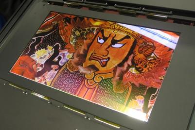
JOLED (Japan OLED) was established in August 2014 by Japan Display, Sony and Panasonic with an aim to become an OLED medium display (10-30 inch) producer. JOLED is using a printing process which should result in lower cost production (but of lower performance displays) compared to evaporation printing.

JOLED/JDI OLED efficiency improvement chart (Jan 2017)

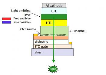
JOLED's R&D Division Manager spoke at the PF&E China conference a couple of weeks ago, detailing the company's process. JOLED is producing RGB-strip OLED panels using ink-jet printers made by Panasonic and PLED materials produced by Sumitomo. The OLED structure is based on Sony's technology and the backplane is a transparent amorphous oxide semiconductor.

Read the full story Posted: Jan 25,2017

Kopin to enter the OLED microdisplay market as a fabless producer

Kopin announced that it is going to enter the OLED microdisplay market for mobile VR and AR applications. The company's first OLED microdisplays will be demonstrated at CES 2017 next month.

Kopin says it has developed a novel silicon backplane structure that will enable high-speed OLED-on-silicon microdisplays. The displays will feature an ultra-high resolution, low power and small form factor.

Read the full story Posted: Dec 21,2016

OTFT developer SmartKem announces a £3 million financing round

UK's SmartKem, a developer of high-performance organic backplanes for flexible displays, announced a 3 million Euro financing round from its existing investors, including BASF Venture Capital, Octopus Ventures and Entrepreneurs Fund.

This new round follows a recent 1.8 million Euro EU grant awarded to SmartKem to support the commercialisation of the company’s technology platform, specifically with display makers in Asia.

Read the full story Posted: Dec 21,2016

The Holst Center developed a Spatial-ALD TFT deposition process

Researchers from the Holst Centre developed a new process to deposit semiconductor layers with better performance and high throughput than PVD-based process. the new process is based on scalable, atmospheric-pressure process spatial-ALD.

Display transistors deposited by sALD image

The Holst Centre used sALD to deposit IGZO backplanes that achieved charge carrier mobilities of 30 to 45 cm2/Vs. The researchers say that similar backplanes deposited with PVD (supttering) achieve about 10 cm2/Vs. The sALD layers also exhibited low off current, switch-on voltages around 0 V and excellent bias stress stability.

Read the full story Posted: Nov 24,2016

SmartKem secured a €1.8 million EU grant to transfer its OTFT platform to display makers in Asia

UK's SmartKem, a developer of high-performance organic backplanes for flexible displays, has secured a €1.8 million EU grant to support the industrialisation and technology transfer of its semiconductor platform to display makers in Asia.

The 2-year project (which will total 2.65 million Euro, with a 850,000 Euro contribution from SmartKem itself) is called FLEXTRANS - and it will accelerate the adoption of organic semiconductors as a universal backplane platform for the mass manufacture of flexible and curved OLED and LCD displays. The project will focus on the industrialisation and transfer of the OTFT platform over large area plastic substrates using standard slit coat processing, while maintaining electrical and physical uniformity and quality of transistor performance.

Read the full story Posted: Sep 06,2016

nVerPix demonstrate its CNT-based OLET displays

In 2011 the University of Florida announced a new organic-TFT backplane/emitter technology called CN-VOLET. The University spun-off the technology into a company called nVerPix, with funding from Nanoholdings.

We have talked to nVerPix in the past and updated on the technology back in 2013. The nVerPix team presented their technology at SID's DisplayWeek - and it won the "best prototype" awarded. nVerPix demonstrate a working mono-color (green) 320x240 2.5" display. The aperture ratio is 70% and the brightness is over 500 nits.

Read the full story Posted: Jun 07,2016

Japan Display to co-develop next-gen CAAC-IGZO backplane tech with SEL

Japan Display (JDI) announced that it has signed a technology development agreement with Semiconductor Energy Laboratory (SEL) regarding the development of Oxide-semiconductor backplane technology for next-generation displays, including OLED displays.

SEL's backplane technology is called c-axis aligned crystal (CAAC), which has been co-developed with Sharp. CAAC is based on an IGZO thin-film that has a novel crystal structure.

Read the full story Posted: May 12,2016

Researchers to demonstrate the world's first CN-VOLET AMOLED prototype

Back in 2011 the University of Florida announced a new organic-TFT backplane technology called CN-VOLET, which is especially suited for OLED panels. Earlier in 2010, the University spun-off a company called nVerPix to commercialize this technology.

At the SID DisplayWeek 2016, researchers from the University of Florida and the University of Seoul will present the world's first AMOLED display panel that use nVerPix's CN-VOLET backplane. The 2.5" monochrome display prototypes features a QVGA (320x240) resolution.

Read the full story Posted: Apr 17,2016

CPT to achieve flexible AMOLED mass production with aid from ITRI

Taiwan's Chunghwa Picture Tubes (CPT) signed an agreement with ITRI for a technology transfer for flexible AMOLED and touch panel integration (specifically ITRI's FlexUP flexible substrate technology - which is owned by FlexUp, encapsulation technology and flexible touch sensor technology).

CPT aims to use these technologies to achieve flexible OLED mass production "as soon as possible". Earlier today we posted that ITRI is set to demonstrate a 7" Full-HD foldable AMOLED prototype soon. ITRI and CPT has been cooperating on flexible OLEDs since 2012.

Read the full story Posted: Aug 06,2015

BOE Display shows four new AMOLED prototypes, including a 9.55" flexible transparent panel

BOE Display is stepping up its OLED program - the company is constructing a 5.5-Gen LTPS fab in Ordos, which will also produce both LCDs and AMOLED displays, it is starting to build a $3.5 billion Gen-6 LTPS LCD/AMOLED production line in Chengdu, and it is also planning a 8.5 OLED TV fab in Hefei Xinzhan.

BOE 9.55'' transparent flexible AMOLED prototype (SID 2015)

Last week BOE demonstrated several new AMOLED prototypes. First up we have a 9.55" flexible transparent panel, which is probably the largest such panel ever demonstrated. It features a resolution of 640x432, a curvature radius of 10 mm and 30% transmittance. The whole panel is just 150 micrometer thick.

Read the full story Posted: Jun 09,2015