Researchers drive an OLED display using Carbon Nanotubes

Researchers from the University of Southern California has created a large functional array of transistors made using simple solution-processing methods from carbon nanotubes. These have been used to drive a simple 4" OLED display, and the group is now working towards a 'truly integrate' OLED display that is both flexible and transparent.

Carbon Nanotubes is a promising material for making control cibruit for displays - they are efficient, and can be used to make flexible and transparent displays. Now the USC researchers have found an 'easy' way to make large arrays of transistors with good performance.

Read the full story Posted: Nov 24,2009

Philips: OLED Lighting will take 3-5 years to achieve good efficiencies

There's an interesting story on Philips Lighting plans over at Tech-On, which obviously includes OLED Lighting. Philips are already shipping samples for quite some time (here's our review). Philips say that currently their OLED has an emission efficiency of 10lm/W to 20lm/W.

Philips OLED panel

They have already achieved 80lm/W "in the lab", but it will take at least 3 years to achieve 50lm/W at the production level, and 5 years to go beyond that.

Read the full story Posted: Nov 23,2009

ARM's new mobile phone reference design includes a WVGA AMOLED display


ARM has presented their "Mobile Client 2010" reference design. Their new chip is the Cortex-A9 dual core CPU - these can be fast - up to 2Ghz, although for a mobile device this will probably be slower. It's not clear yet whether these chips will be ready for production in 2010.


The design also includes the ARM mali 400MP GPU and the screen of choice is a WVGA AMOLED.

Read the full story Posted: Nov 20,2009

UDC and the FDC enhance their collaboation on flexible OLEDs for the US army

Universal Display (FDC) and the Flexible Display Center (FDC) at Arizona State University announced that they have strengthened their collaboration to extend to the joint fabrication of prototype active-matrix PHOLEDs on flexible plastic substrates for the U.S. Department of Army. In addition, Universal Display announced that the company has been awarded a $650,000 U.S. Army Small Business Innovation Research (SBIR) Phase II Enhancement contract to support this work.

UDC and the FDC believe that the enhanced relationship will accelerate the demonstration of the flexible AMOLEDs. Earlier in 2009, they have already demonstrated a 4.1" monochrome QVGA PHOLED display.

As part of this strategic relationship, Universal Display and the FDC will work to demonstrate flexible OLED display prototypes with enhanced performance for the U.S. Army. The FDC will fabricate a-Si:H thin-film transistor (TFT) arrays on flexible plastic substrates using their low-temperature backplane and proprietary bond-debond manufacturing technologies. Universal Display will then use its UniversalPHOLED materials and technology to build full-color AMOLED displays

For prototypes to be delivered under the U.S. Army SBIR Phase II Enhancement Program, Universal Display will also use its proprietary encapsulation film technology to create permeation barriers on the substrate and on top of the OLED to prevent harmful moisture and oxygen from reaching the OLED device.

Read the full story Posted: Nov 20,2009

Rumors: Apple delays its tablet for 2H10, and there will be an option for a 9.7" OLED

There are new Apple-OLED-tablet rumors, this time from Digitimes, which might make it true this time. Apple are said to postpone their tablet PC to 2H 2010. There will be two models - one with a 10.6" TFT LCD, and one with a 9.7" OLED. The OLED will be made by LG Display.

Digitimes also say that a 9.7" OLED panel will cost about $500 US today, which is very expensive for such a gadget. However OLED Prices are expected to fall rapidly, and so the final price of the tablet should be around $1,200 to $1,500, and could be lower if it's bundled with 3G services. The LCD tablet is expected to priced at about $800-$1,100.

Read the full story Posted: Nov 19,2009

The Fraunhofer institute and Philips are working on a new way to apply OLED conductor paths


The Fraunhofer Institute for Laser Technology (ILT) is developing a new cost-efficient process for applying conductor paths to OLEDs. The new process also makes homogeneous luminosity for the OLED panels, thanks to micro-scale conductor paths.


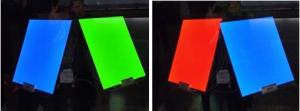
When you make OLEDs, you apply metallic conductor paths to the anode layer (ITO - Indium Tin Oxide - or similar materials). The size of these conductor paths plays an important role here: if they are too wide the paths can affect the luminous homogeneity of the light source. Today the metallic conductor material has been applied to the OLED surface using a vacuum sputter process which is energy intensive, has up to 90% material loss and is expensive. It is also not environmental friendly as it uses metals that has to be disposed of after use. The conduct paths are wide, and so disrupt the homogeneous luminosity of the OLEDs.


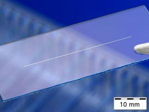
The Fraunhofer ILT is now developing a laser technique to apply
micro-scale conductor paths for the industrial partner Philips. A mask
foil is placed on the surface of the conductor which represents the
negative to the conductor path geometry later required. This is then
covered by a donor foil whose material will constitute the conductor
path, for example aluminum or copper. The assembly is fixed in place
and hit with laser radiation traveling at a speed of up to 2.5 m/s
along the mask geometry. A mixture of melt drops and vapor forms, which
is transferred from the donor foil to the substrate. The solidified
mixture produces the conductor path, whose geometry is determined by
the mask. As the process takes place in the ambient atmosphere an
expensive process chamber is not required. There is no material loss
because the residual material of the donor foil can be re-used.


More information here


Read the full story Posted: Nov 19,2009