The following is a guest article, by Assaf Levy-Beeri, Co-founder at Joya Team
MicroDisplays are used in a variety of applications. First introduced into the market in the 90s, microdisplays were used as an image source for Rear Projection TVs (RPTVs), projectors, viewfinders for digital cameras and Helmet Mounted Display systems (HMDs).
Today, while the demand for wearable products is increasing and the potential wearable market size is very high, microdisplay market is expected to grow dramatically. Augmented Reality (AR) and smart glasses, Helmet Mounted Displays , Virtual Reality (VR) systems and Head-Up Display (HUD) systems are the main applications where a high-resolution microdisplay is required. Correspondingly, the technology is improving all the time and microdisplays manufacturers make significant investments in order to improve their technology and products performances. In addition, new technologies and manufacturers enter this field.
The Microdisplays market size is estimated to have reached around $1 billion in 2018 and is expected to grow to ~$3.5 billion by 2024, at a CAGR of about 25%. The increasing adoption of HMDs in a variety of applications in different markets, such as military (avionics, simulators, field combat), medical, automotive, consumers and entertainment, is expected to drive the microdisplays market growth in the upcoming future.
Microdisplays Technologies
The basic definition of a microdisplay is an ultra-small display size (less than 1’’ diagonal). In most cases, the resolution of the microdisplay is high and the pixel size is usually 8 to 15 microns. Therefore, microdisplays are often used with magnifying optics like in AR or HUD case There are 3 main types of microdisplays:
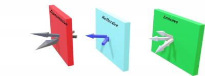 Figure 1 : Microdisplay types
- Transmissive: light is passing through the microdisplay. Image is formed by the interaction of light, liquid crystal and color filters. In most cases, transmissive microdisplay will be an LCD panel where each pixel is addressed to control light polarization.
- Reflective: light is reflected from the microdisplay. Image is formed by modulation and reflection of light from the pixels. Reflective microdisplays may make use of liquid crystals and polarized light as in LCoS case, or, as in DLP case, light is reflected from controlled micro-mirrors, where each micro-mirror represents a pixel and this way the image is created.
- Emissive: light is emitted from each pixel as a result of current or voltage supply. Image is formed by the light emitted by each pixel at different luminance levels and colors. Examples of emissive microdisplays are OLED, Micro-LED and CRT.
In the next paragraphs, I will present a brief overview of the main Microdisplay technologies on the market with a focus on full-color microdisplays rather than monochrome.
Liquid Crystal Display (LCD)
The basic structure of an LCD panel is a liquid crystal (LC) layer placed between two transparent electrodes and two crossed polarizers. In most cases, the LCD microdisplays are twisted nematic. In TN LC, at its basic state, the liquid crystal molecules are aligned so that this structure induces phase retardation when light goes through it, resulting in a polarization rotation of 90 0 . This kind of LCD is also called normally open, to point out that when no voltage is applied, the LCD will present a white image (open state or "on
state").
In "on state" (no voltage is applied to the LC), the light entering the panel passes through a polarizer and becomes linearly polarized, then interacts with LC molecules which causes a polarization rotation of 90 0 . Then, the light passes through the second polarizer (analyzer), which is aligned perpendicularly to the incident polarizer. In "off state", when a voltage is applied between the electrodes creating an electric field, the LC molecules are arranged so that the light polarization is not affected. The incident light passes through the linear polarizer, then passes through the LC with no effect on polarization, and finally passes through the perpendicular polarizer that absorbs all of it. The result is that no light is transmitted through the LCD.
These two states of LCD represent a white and a black image, respectively. Grey levels are achieved when applying a mid-level voltage (electric field), and by that tuning the retardation effect on light polarization causing partial absorption of light by the analyzer.
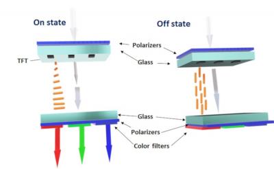
Figure 2 : LCD operation principle
As discussed above, LCD is a light modulator, that requires a light source, or a backlight, in order to create an image. This backlight shall be designed in conjunction with the optical system considering the specific LCD performances. A smart backlight design, considering system requirements and LCD limitations, such as polarization, color space, maximum luminance limitation, LC temperature sensitivity, viewing angles, LCD transmission and extinction ratio, system’s limited dimensions and others, results in optimal system performances with the given LCD panel and allows to save power.
Liquid Crystal on Silicon (LCoS)
An LCoS is a reflective display, based on Liquid Crystal. A CMOS backplane controls the voltage applied to the LC, on a reflective electrode. Like in transmissive LCD, the LC arrangement in LCoS panel also controls the polarization of light passing through it. The LCoS is also a light modulator, which utilizes polarization and requires a light source in order to project an image. A typical LCoS projection unit is presented in the next figure.
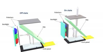 Figure 3 : LCoS projection unit scheme
An RGB backlight projects unpolarized light through a polarizer. The resulting linear polarized light (S-polarization) is then reflected from a Polarizing Beam Splitter (PBS) towards the LCoS panel (The PBS reflects S-polarization part of the incident light and transmits P-polarization part). Then the S-polarized light is incident on the LCoS panel.
In the "off state" the LC has no effect on the polarization orientation. The linear S-polarization is reflected from the LCoS panel and the PBS reflects it back towards the backlight, so no light gets out of the projection unit.
In the "on state", the LC has a retardation effect similar to quarter waveplate. The linear S-polarization is changed into right-handed circular polarization. Then it is reflected from the LCoS reflecting electrode and changed into left-handed circular polarization. Another passage through the LC changes the polarization from right-handed circular into linear polarization, 90 0 to the incident polarization (P- polarization). The light then is transmitted through the PBS and through the second polarizer (analyzer) with the proper orientation to transmit the P-polarization and a white image is presented.
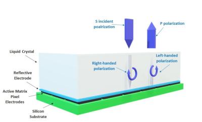
Figure 4 : LCoS panel polarization principle
These two states of LCoS represent a black and a white image, respectively. Grey levels are achieved when applying a mid-level voltage (electric field), and by that tuning the retardation effect on light polarization causing partial absorption of light by the analyzer.
Another option to produce grey levels in LCoS is toggling between on and off states in duty cycles. This can be done only at a very high frame rate, like in a ferroelectric LC. Full-Color image in AR systems is produced sequentially by synchronization between RGB backlight (may consist of LEDs or Laser diodes) and the image on LCoS panel.
Digital Light Processor (DLP)
DLP is a display device developed by Texas Instruments. This device is an array of micro-mirrors, each one representing a single pixel of the displayed image. Each micro-mirror can be electrostatically tilted into two positions: +120 and -120 . (in advanced architectures there is also ±17 0 tilt, giving better power efficiency of projectors).
A DLP projection system also requires an RGB light source in order to produce a full-color image. An illuminated mirror tilted at +120 , produces "on state" pixel, and a mirror that is tilted at -120 , direct the reflected light into an absorbing area, producing "off state" pixel. Greyscales are achieved by tilting the micro-mirrors at different duty cycles, and colors are produced by color sequential method synchronization between the RGB light source and micro-mirrors.
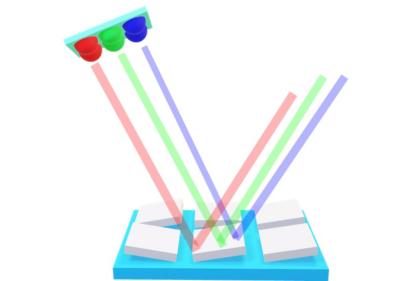 Figure 5 : DLP operation principle
There are a few AR products and prototypes using DLP devices as an image source. However, it is a challenging design that requires special attention to issues related to the systems’ Etendue. There is a considerable trade-off between key parameters, such as FOV and exit pupil size as well as system’s efficiency, brightness, contrast and size.
Organic Light Emitting Diode (OLED)
OLED Microdisplay is a solid-state emissive electroluminescence device, consisting of an organic layer, which is placed between two electrodes and emits light as a result of electric current. The OLED basic structure is presented in the next figure.
 Figure 6 : OLED structure
When applying a voltage across the device, the transparent anode (commonly ITO layer) is kept positive with respect to the cathode. A current of electrons passes through the device from the cathode through the Electron Transport Layer (ETL) to the emissive layer. This electron current is captured by the emissive layer causing the anode to withdraw electrons from the conductive layer or Hole Transport Layer (HTL), which occurs as a flow of holes in the conductive layer.
Electrostatic forces drive the electrons and the holes towards each other and they recombine (close to the emissive layer) forming excitons. The relaxation of this excited state causes the electron to drop to a lower energy level, which is accompanied by the light emission with a frequency depending on the band gap of the emissive material.
An OLED microdisplay has many advantages for AR systems. It doesn’t require any backlight and that makes it optimal for integration in the optical system. Another advantage of the OLED is that it has an excellent image quality, it is very efficient comparing to LCD or LCos for example [Lumens per Watt] and has an ultra-high CR and wide color space. On the other hand, the OLED has limited luminance and limited lifetime. That makes it marginal for applications that require very high luminance level, especially for outdoor applications when a color image is required, with a reasonable lifetime.
MicroLED
MicroLED is an emerging display technology that has a great potential to replace other Microdisplay technologies and become the leading technology for image source for AR and HMD systems.
A microdisplay based on microLED technology is aimed to provide all the advantages of an OLED microdisplay: simplicity in systems design and integration, ultra-high CR, wide color space, low power consumption and small form factor, with the added values of very high brightness level and wide color Gamut.
The microLED microdisplay is based on a standard Gallium Nitride (GaN) wafer, adopted from standard LEDs industry. This approach has the potential to provide high luminance display device without lifetime issues at a relatively low price.
In general, the standard GaN wafer is patterned into arrays of micro-LEDs. The microLED display is then produced by an integration of microLED array and transistors. There are several approaches being developed by different companies and research institutes in the last couple of years:
- Pick-and-place: In this approach, the MicroLED units are transferred from the wafer to the transistor backplane. In order to produce a high-resolution microdisplay, it's required to transfer several millions of LEDs with an accuracy of around 1 um. This approach is not feasible commercially and technologically for microdisplays since the required accuracy is too high, it takes a lot of time to transfer millions of LEDs with this accuracy and the yield is potentially low. Medium and large area displays manufacturers are dealing with those issues and developing new methods to make it feasible, cost-effective and scalable to serial production.
- Flip-chip bonding: In this approach, the microLED array and CMOS transistors are fabricated separately. Then, both wafers are assembled and bonded together. The advantages of this approach are improved heat dissipation and light extraction. The alignment accuracy of microLED with CMOS using this approach is also improved and prototypes with high resolution of 10 microns pixel size have been produced. However, the accuracy is still limited since in order to generate color microdisplay it is required to reduce the sub-pixel size to 3-5 microns. So this approach is suitable for monochrome displays and not for full-color displays.
- Monolithic integration of transistors on MicroLED array: Monolithic structure of microLED microdisplays is becoming the leading and the most promising approach for microLED-based microdisplay development. The production is done directly on the GaN wafer by fabrication of TFTs, on each of the microLEDs pixels. No transfer is involved in this approach. The monolithic approach is using standard CMOS manufacturing processes and is scalable to standard 200mm wafers. It has a great potential to enable smaller pixel sizes and high-resolution microdisplays.
The microLED development for microdisplays is still going on. There are several companies that are exploring and developing this technology. Several demos have been presented in 2018 and 2019, and first products are expected to go to market by 2020-2021. Still, there are some technical challenges that need to be addressed
- Shrinkage of pixel size: 3-5 microns pitch is required
- Color Generation: development of Full-color microLED based on a single color LED wafer
- Spatial uniformity of microLED display due to variations of color and luminance between microLED chips
- Integration of a sustainable product (new product labor pains): like any other novel technology, the current experience with integration of this technology into a product on a display level and on a system level is limited. According to our experience, it takes years until a display technology becomes mature enough and manufacturers overcome all initial challenges. We expect the integration issues to occur in microLED technology.
To conclude all the stated above, it’s obvious that microLED-based microdisplays may solve some of the main issues and bottlenecks of the AR systems, however, it may take a significant time and effort until it can be used in AR systems and replace current microdisplay technologies, providing all the expected performances at a reasonable lifetime and price.
Summary: MicroDisplays Technologies used in AR systems
The selection of the microdisplay to be used in an augmented reality system has a major impact on systems performances. It determines the systems parameters, such as see-through contrast (display luminance), curtain effect (display contrast ratio), uniformity, color space, exit pupil size and system resolution. Microdisplay also has a significant impact on system size, weight and cost.
Therefore, it’s highly important to understand the differences between microdisplays technologies and to take into account the advantages and drawbacks of each technology. An optimal selection and the implementation of the microdisplay may differentiate the display system from its alternative and provide good performances at an acceptable volume and cost. Sometimes during the development of AR or HUD system, the developers prefer or choose to design the optical imaging system first and only then add a microdisplay using any available technology. It may work in some cases for some extent, but in most cases, the system will not be optimal and will fail to meet the requirements or the customer’s satisfaction.
In JOYA Team we believe that the image source is a part of the design of the system, starting at the integration of the requirements all the way to the product. We believe in working together and cover all systems aspects: System Engineering, Optical Design, Non-Imaging Design, Human Factors Engineering, Hardware, Mechanical Engineering, Heat Dissipation, Lifetime, Material and more, in order to get the optimal display system.
References
- https://www.marketsandmarkets.com/PressReleases/microdisplay.asp
- http://www.ti.com/dlp-chip/getting-started.html
- http://www.plesseysemiconductors.com/wp-content/uploads/Plessey-MicroLEDs-White-Paper-1.pdf
About the Author:
Assaf Levy-Be’eri is a physicist and optical engineer with expertise in non-Imaging and microdisplays technologies for Augmented Reality systems. He is also a Co-founder of JOYA Team - an Optical Technologies House offering optical systems’ development services with expertise in AR and VR optical systems.
JOYA Team designs optical systems using a unique development methodology that creates an optimal working point, incorporating a holistic approach, including imaging & non-imaging design, new electro-optics and display technologies, in addition to testability, manufacturability, cost and other system aspects.
For more information, please visit our website: www.joyateam.com

