V-Technology to start producing next-generation OLED fine metal masks, acquires OLED lighting maker Lumiotec

V-Technology announced that it is establishing a new organic electronics subsidiary that will develop a next-generation OLED deposition technology that V-Technology refers to as fine hybrid mask (FHM). Total investment in this new company is estimated at 5 billion Yen ($46 million USD) for the next 2-3 years. The facility is scheduled to be completed in August 2018 and V-Technology will start shipping mask samples in October 2018.
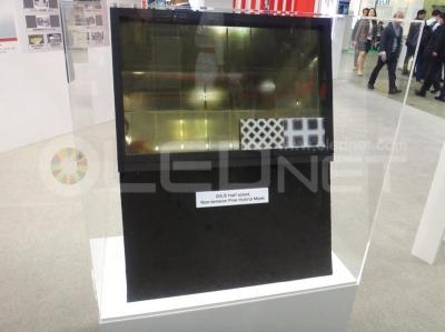
V-Technology FHM mask demonstration (Feb 2018)

V-Technology's FHM is based on an electroforming method and the masks have a non-tension structure. V-Technology says that the total mask weight will be one tenth of current regular FMM masks, which will lower bending dramatically. V-Technology's already demonstrated an FHM that achieves 738 PPI.

Read the full story Posted: Feb 11,2018

CPT and imec demonstrate an 1250 PPI OLED patterned using a photolithography process

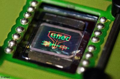
Taiwan-based Chunghwa Picture Tubes (CPT), in collaboration with European research institute imec (in the framework of the Holst Centre collaboration) have demonstrated an ultra-high resolution OLED display that was patterned using photolithography - without the need for an FMM (metal mask). A photolithography process offers a high aperture ratio, large substrate sizes and good yield control.

FMM-free photolithography-made OLED prototype (CPT + imec)

The prototype display that was demonstrated is a passive display with a 1400x1400 resolution (or 1250 PPI!) of side-by-side orange and green OLEDs. imec reports that preliminary lifetime investigation shows operation of each color after patterning for a few hundred hours at more than 50% of the original brightness.


Read the full story Posted: Sep 20,2017

AP Systems achieves 1000 PPI with new FMM technology

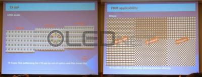
At the iMID 2017 conference in Korea, AP Systems announced that it realized high density OLED evaporation using new FMM technologies. By adopting ultra-short pulse laser (USPL), AP Systems achieved a 1,000 PPI. Changing the pin-hole shapes, the company says this technology can even reach 1,170 PPI.

AP Systems 1000 PPI slide (IMID 2017)

High PPI OLEDs are especially important for VR applications, which require much higher pixel densities as the display is used very close to the eye. In May 2016 Samsung demonstrated a 5.5" 3840x2160 - which reaches 806 PPI, and according to reports Samsung were able to produce a 1,200 PPI AMOLED in March 2017.

Read the full story Posted: Sep 05,2017

IHS: the AMOLED FMM market will reach $1.2 billion in sales in 2021

Analysts from IHS say that as AMOLED displays continue to replace LCD displays and the AMOLED market is growing quickly - the market for fine metal mask (FMM) components will also experience fast growth in coming years.

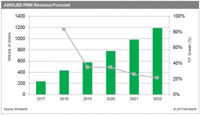
AMOLED FMM revenue forecast (2017-2022, IHS)

IHS sees the FMM market in 2017 generate $234 in revenues. The market will grow at a compound annual growth rate (CAGR) of 38% until 2022 - to reach $1.2 billion. IHS says that FMM production is a challenge and FMM technology has become a bottleneck as display resolution is increasing and the number of FMM suppliers is limited. The leading producer is Dai Nippon Printing, and the company's FMM masks are using to produce the majority of AMOLED displays.

Read the full story Posted: Jul 18,2017

Dai Nippon Printing to supply FMM masks to BOE Display

According to ET News, Japan's Dai Nippon Printing (DNP) has terminated Samsung's exclusivity for the company's fine metal masks (FMM) products. DNP is now offering its masks to other OLED makers, and have already signed up BOE Display as a customer.

DNP has advanced its FMM technology, and is now able to produce masks with high resolution - enough to create QHD (2560x1440) smartphone displays. BOE's current masks only enable it to produce FHD OLEDs, and it will now upgrade its production to higher-end displays using DNP's masks.

Read the full story Posted: Jun 20,2017

Samsung's Gen-7 A4 flexible OLED line to be ready by Q2 2018

According to reports from Korea, Samsung has started construction of a new flexible OLED fab, which will be called the A4 line. This will be Samsung's first Gen-7 line as the company is aiming to expand its technology gap over its upcoming OLED competitors who are all building Gen-6 line.

A Gen-7 line substrate is 1870x2200 mm in size - as opposed to 1500x1800 mm for Gen-6. This means that you can produce more displays per substrate and price per screen is lower. Scaling up evaporation OLED production is not so easy, but it seems that Samsung managed to solve its technologies hurdles - mainly the FMM metal masks and the LTPS annealing process.

Read the full story Posted: Apr 20,2017

Sunic Systems managed to achieve 1,500 PPI Using plane source evaporation

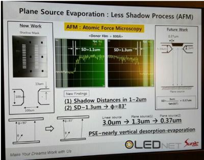
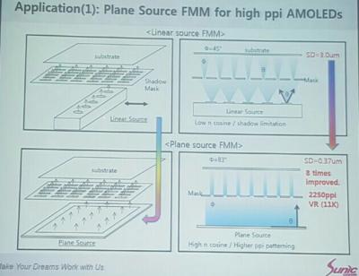
Sunic System recently unveiled a new evaporation-FMM based AMOLED system that enables high resolution deposition - Sunic says it will enable PPI up to 2,250 PPI. Sunic's new technology makes use of a plane source for evaporating OLED materials, as opposed to the currently-used linear source. Such high resolution displays will be very useful for VR applications.

Sunic: plane-source evaporation (Nov-2016 slide)

Sunic System now announced that it succeeded in implementing 1.1um shadow distance by using the new plane source evaporation and 100um shadow mask. Such a small shadow distance can achieve 1,000 to 1,500 PPI resolutions. The company's next step is to lower shadow distance to 0.37um - which will indeed enable 2,250 PPI and 11K high-resolution mobile AMOLEDs.

Read the full story Posted: Nov 11,2016

Korean-based DAWONSIS suggests a new FMM-based method for large-area OLED deposition

Korea equipment maker DAWONSIS developed a new OLED deposition process that is based on FMM but according to the company can be scalable to large-area deposition. This could theoretically enable efficient evaporation-based OLED TV production.

DAWONSIS Joule Heating Deposition photo

The so-called Joule Heating Deposition process use a large area material source (as opposed to point-sources or line-sources currently used) using a conductive film that is efficiency heated using voltage induction. According to DAWONSIS this process is scalable and also efficient in terms of material usage (which is about 70%-80%).

Read the full story Posted: Sep 14,2016

Sunic System's plane-source technology enables 2,250 PPI AMOLEDs and FMM OLED TV production

One of the key requirements for VR application is high-density displays, as small-sized displays are magnified to cover our whole field of view. Some estimate that realism VR demands around 2,000 PPI.

Sunic System plane-source FMM slide

During SID 2016, Samsung announced it developed a 806 PPI AMOLED especially for VR application. This is an upgrade from current OLEDs, but still a far cry from the 2,000 PPI mentioned above.

Read the full story Posted: Aug 30,2016

Innolux shows new rigid and flexible OLED prototypes, aims to mass produce AMOLEDs

After years of OLED R&D but no actual reports, Taiwan's Innolux is finally demonstrating its new OLED prototypes, signalling that the company is finally about to re-enter the OLED market. Innolux says that it has recently "achieved success with AMOLED technology" and now plans to continue development and ultimately mass produce AMOLED panels.

In a trade-show in Taiwan, Innolux is demonstrating several OLED prototypes. First up we have a 5.5" WQHD (2560x1440, 534 PPI) flexible AMOLED built on a plastic substrate and an LTPS backplane. The panel has a "proprietary pixel rendering methods" (perhaps PenTile like?) and uses thin-film encapsulation and is produced using an FMM mask (more on this below).

Read the full story Posted: Aug 23,2016