![]() Japan-based Semiconductor Energy Laboratory (SEL) is an R&D IP company founded in 1980. SEL performs R&D in several areas, including transistors and semiconductor devices, materials and devices for OLEDs and batteries, display devices and more.
Japan-based Semiconductor Energy Laboratory (SEL) is an R&D IP company founded in 1980. SEL performs R&D in several areas, including transistors and semiconductor devices, materials and devices for OLEDs and batteries, display devices and more.
SEL is actively researching and developing flexible OLED technologies. Over the past years, the company announced partnerships with Nokia, Japan Display and Sharp.
In 2019 SEL demonstrated its latest OLED technologies - including foldable and high-density displays.
398 Hase,
Atsugi-shi,
243-0036
Japan
Will SEL's ExTET device architecture finally enable an efficient blue OLED?
Researchers from Japan's Semiconductor Energy Laboratory (SEL) developed a new OLED device architecture that enables efficient, long-lasting and low-drive voltage OLEDs, at practical brightness levels.

The researchers call the new device architecture exciplex-triplet energy transfer, or ExTET. The image above shows the elementary process and its energy state diagram. To create the emissive layer of the ExTET, the researcher took a film with an electron-transporting material (ETM) and a hole-transporting material (HTM) and doped it with a phosphorescent dopant. Direct recombination between the electrons at the LUMO level and the hole at the HUMO level forms a charge-transfer excited complex (exciplex) - and the phosphorescent emission occurs via energy transfer from the exciplex to the dopant.


SEL demonstrated its TR-hybrid OLED/RLCD display
In April 2016, Japan's Semiconductor Energy Laboratory (SEL) and Advanced Film Device announced they have developed a hybrid OLED - reflective LCD display, that can switch between an OLED mode (for dark environments) and reflective LCD mode (for sunlight visibility). Such a display could be very power efficient.
 TR-Hybrid in OLED mode
SEL demonstrated a prototype display at SID 2016, and provided more information. SEL calls these displays TR-Hybrid displays (TR means Transmissive OLED and Reflective LC). To create this display, SEL introduced holes into the reflecting electrodes of a reflective LCD, and the OLED layer beneath transmitted light through these holes in OLED mode.
Japan Display to co-develop next-gen CAAC-IGZO backplane tech with SEL
Japan Display (JDI) announced that it has signed a technology development agreement with Semiconductor Energy Laboratory (SEL) regarding the development of Oxide-semiconductor backplane technology for next-generation displays, including OLED displays.
SEL's backplane technology is called c-axis aligned crystal (CAAC), which has been co-developed with Sharp. CAAC is based on an IGZO thin-film that has a novel crystal structure.
SEL developed a hybrid OLED - reflective LCD display
Researchers from Japan's Semiconductor Energy Laboratory (SEL) and Advanced Film Device developed a display that includes an OLED display on top of a reflective LCD. The idea is that such a display have high visibility in both a dark environment (using the emissive OLED) and a bright one (using the reflective LCD).
This is similar somewhat to transflective LCD displays and can prove to be a smart solution. The researchers say that the same FET layer is used to control both display devices and so results in a low-power device. The researchers will present this new development at SID DisplayWeek next month and hopefully we will bring more information.
Photo reveals SEL's 81" 8K tiled OLED display is not really seamless
Last week Japan's SEL demonstrated an 81" 8K OLED display, built from 36 13.5" flexible OLED panels that have transparent edges on two adjacent sides. The panels are tiled together seamlessly - and this enabled SEL to create the world's largest OLED display ever.

We now have a photo of the display prototype, as you can see above. While this is an impressive feat, it's quite clear that the display is not seamless and you can say the places where the tiles are connected.
81" 8K OLED display developed using seamless flexible OLED tiles
Researchers from Japan's Semiconductor Energy Laboratory (SEL) and Advanced Film Device developed a 81-inch 8Kx4K OLED display that is built from 36 13.5" flexible OLED panels that have transparent edges on two adjacent sides.
The transparent edges enabled the researchers to connect the tiles seamlessly - to create the world's largest OLED display ever developed.
SEL shows a 8.7" FHD touch tri-folded AMOLED prototype
In June 2014, Japan's Semiconductor Energy Laboratory (SEL), in collaboration with Nokia, unveiled new foldable OLED display prototypes - 5.9" 1280x720 (249 PPI) ones, which can be folded in two or in three (these were two different prototypes).

Last month in Japan SEL unveiled new prototypes. The new panels are bigger at 8.7" and offer a higher resolution (1920x1080, 254 PPI). The new panels are also touch-enabled. And they are still tri-folded like the ones shown in June.
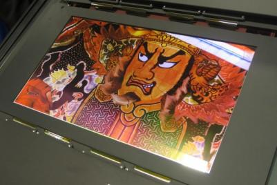
SEL and sharp show a 13.3" 8K (664 PPI!) AMOLED prototype
As we reported back in February, SEL and sharp unveiled a 13.3" 8K OLED prototype. This ultra high density (664 PPI!) display uses SEL's C-axis-aligned crystalline oxide semiconductor (CAAC-OS) backplane.
SEL's previous 13" CAAC-OS OLED prototype featured 326 PPI. But that lower-resolution panel was flexible. This new panel uses white OLEDs with color filters. SEL adopted micro cavities to narrow the wavelengths. The display features a 84% NTSC color gamut (rather low for an OLED). Each OLED pixel is driven by five transistors and one capacitor (5T+C) - there are almost 500 million pixel transistors in this display.
SEL and Nokia developed foldable OLED prototypes
Semiconductor Energy Laboratory, in collaboration with Nokia developed a new foldable OLED display. The companies are demonstrating two display prototypes. Both displays are 5.9" in size with a 1280x720 (249 PPI) resolution. One of them can be folded in two (like a book) and the other can be folded in three (seen in the video below).
Those flexible OLED displays use a white OLEDs with color filters (WOLED-CF) design. To produce the display, SEL deposited the organic and color filters layers on a glass substrate, which is later peeled off and replaced with a flexible substrate. The displays can be bent up up to a curvature of 2 mm (two-folds) or 4 mm (three folds). SEL says that these displays can be bent more than 100,000 times.
New OLED development to be discussed at SID 2014
The SID Display Week, the world's leading display industry showcase is scheduled for June, but the organizers already published the list of papers to be presented in this show. Hiding in this long list of technical achievements and research projects are some interesting new OLED developments. So here's some of the achievements to be announced during the show (at no particular order).
TCL's China Star Optoelectronics Technology (CSOT) managed to fabricate a 7" QVGA (320x240) flexible PMOLED display. The display uses a thin PEN substrate, processed at Gen-4.5. The company also proposes a design for a 14" QVGA PMOLED panel. CSOT also developed a 31" Full-HD AMOLED panel that uses a IGZO backplane. The 31" direct-emission panel was produced on a Gen-4.5 glass substrate using FMM.