A few months ago we reported on research conducted at Germany's Max Planck Institute, led by Prof. Paul W.M. Blom, that looks into single-layer OLED devices. In such devices, a single TADF OLED emitter layer is sandwiched between two electrode - a much simpler design compared to commercial OLED devices that use multilayer stacks, sometimes with 10 or more layers.
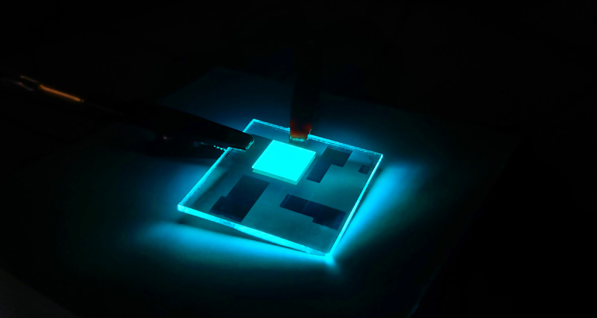
The researchers the the MPI say that in fact it is possible to develop highly efficient OLEDs with just the TADF emitter, as there's no fundamental reason or major benefits that arise from multilayer OLEDs. The researchers continue their work, and now they have developed a new single-layer blue OLED in which every injected electron is converted into a photon - or 100% IQE. This is the first time that such a single-layer OLED device was demonstrated (see image above).
The new device exhibits an external quantum efficiency of 27.7%, with minor roll-off at high brightness. The loss in efficiency is due to light outcoupling, as the internal efficiency is almost 100%.
The OLED device consists of a layer of a TADF emitter blended with a host in equal ratios, sandwiched between a PEDOT:PSS:PFI hole contact and a metal top electrode, without any additional interlayers. It was verified that these contacts provide ohmic charge injection. This proves that a highly simplified, single-layer OLEDs with zero electrical losses are a feasible alter-native to state-of-the-art multilayer devices.
This research could have far-reaching implications, as it could lead to lower-cost OLED production, which requires only the emitter and the electrodes without the deposition of other layers. The next step for the researchers is to improve the stability (lifetime) of the device, and also improve the light outcoupling.
Prof. Paul W.M. Blom told us that once the device performance improves, the researchers aim to look into possible industry commercialization. He also explains that the researchers chose a TADF emitter rather than a PHOLED one because the PHOLED emitter acts as a charge trap, thereby destroying the charge transport and balance. In a TADF emitter the transport and triplet harvesting is on the same molecule. For a multilayer device the trapping is not so relevant since the emissive layer is very thin - but for a single layer device this is critical.

