OLED (Organic Light Emitting Diodes) is a flat light emitting technology, made by placing a series of organic thin films (usually carbon based) between two conductors - and these films light up when electrical current is applied. OLEDs are used to make display and lighting panels. OLED displays an offer excellent image quality, are thinner, more efficient than LCD displays, and they can be flexible.

One of the major problems with those organic materials is that they are very sensitive to oxygen and moisture. This means that OLEDs need to be protected - as even a single water or oxygen molecule can harm the OLEDs.
Thin Film Encapsulation (TFE)
With regular (rigid) OLED panels, one can use a glass sheet. Glass is a great barrier, and it is widely used in the display industry and so easy to handle.
For flexible panel, rigid glass is not a a good option, and in such panels producers use different techniques, collectively referred to as Thin Film Encapsulation, or TFE. TFE is a multi-layer film, made from alternating organic and inorganic layers.
Most organic layer TFEs use an inkjet printing process. Inkjet printing is used to deposit the organic TFE materials. Kateeva launched an encapsulation inkjet printer system towards the end of 2014, and in 2016 the company announced that it secured the "vast majority" of available TFE orders.
The inorganic TFE material deposition can be done in different methods. The incumbent technology for the inorganic TFE deposition is Plasma-enhanced chemical vapor deposition (PECVD) while Atomic Layer Deposition (ALD), a modification of the basic CVD process, seems to be gaining ground in the TFE market as it enables thinner and more uniform films.
Further reading
The latest OLED encapsulation news:
The Holst Centre developed and demonstrated a new barrier for foldable OLEDs
The Holst Centre is demonstrating a new optimized encapsulation (barrier) layer for foldable OLED panels. The new barrier is made from an organic layer sandwiched between two layers of silicon nitride (SiN). These are standard materials, but by optimizing the stack design the researchers at the Holst Centre were able to control its mechanical properties and create a much more flexible barrier.
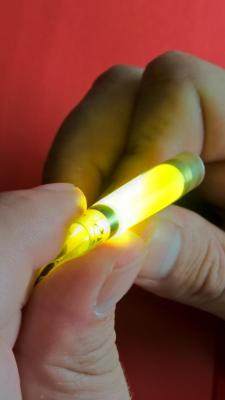
The Holst researchers used an organic material that can withstand 400 °C and can be applied by slot-die coating. This allows the SiN layers to be deposited at 350 °C, improving their quality and ability to prevent water penetration. The Holst tested the OLED prototypes that use the new barrier for 1,000 hours (in accelerated lifetime testing) and no black spots appeared, even after 10,000 folding cycles (bending radiud 0.5 mm).
Graphene-based barrier demonstrated as a possible solution for flexible OLED encapsulation
Graphene is the world's most impermeable material, and as the material is also transparent, flexible and ultra-thin it makes sense to adopt graphene as an encapsulation layer for next-gen OLED displays. A UK project led by Cambridge University researchers have set out in 2015 to develop such a solution, and the researchers now report that they have demonstrated a viable graphene solution comparable to existing commercial OLED encapsulation technologies.
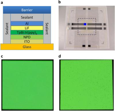
In its pure form, graphene is permeable to all gases, but real life materials are never entirely pure and defects and holes harm the material's permeability. The new research used ALD and CVD to create large-area high-quality single-layer graphene sheets which were stacked to create a multi-layer coating. The researchers say that a ~10 nm barrier layer that includes 3-4 layers of graphene (with AlOx in between) is an effective solution for OLED displays. The 10 nm layer maintains a high optical transparency (>90 %) and high flexibility.
Idemitsu Kosan and Toray to co-develop OLED materials
 Japan-based OLED material maker Idemitsu Kosan announced a new partnership with Toray Industries to co-develop OLED materials.
Toray and Idemitsu will mutually utilize the OLED materials, technology and expertise that both companies possess, and will cooperate in the development of new materials and material evaluation. The two companies will also jointly use their evaluation facilities and production facilities. Both companies hope that this collaboration will accelerate OLED material development and enable lower cost production.
The Fraunhofer FEP, NSMAT and MSSMC developed an OLED on a stainless steel substrate
The Fraunhofer FEP institute, in collaboration with Nippon Steel & Sumikin Materials (NSMAT) and Nippon Steel & Sumitomo Metal Corporation (NSSMC), developed a new OLED lighting prototype that is made on a stainless steel substrate.
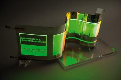
The researchers say that a stainless steel substrate has several advantages compared to glass or plastic - it has excellent thermal conductivity and excellent barrier properties. The lighting panel features an extremely homogenous OLED light, thanks to the planarization layer developed by NSSMC. The prototype panel was produced at the Fraunhofer's R2R research line.
CSoT orders OLED deposition equipment from AP Systems for its 6-Gen flexible AMOLED fab in Wuhan
AP Systems announced that it has received orders for OLED deposition equipment from CSoT for the company's 6-Gen flexible AMOLED fab in Wuhan that is currently under construction.
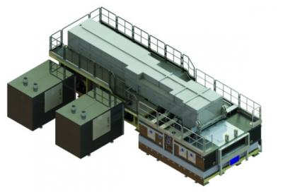
AP Systems said that the whole order is worth $60.65 million and the equipment will be delivered starting in September 2017 until October 2018. AP Systems did not disclose the equipment list, but the company's main products are laser annealing equipment (used to produce LTPS substrates), laser list-off equipment and OLED encapsulation tools.
IHS: The OLED encapsulation material market will grow at a 16% CAGR to reach $233 million by 2021
According to IHS, the OLED encapsulation material grew 4.7% in 2017 to reach $117 million. IHS expects the market to grow at a 16% CAGR to reach $233 by 2021.
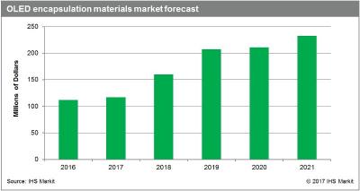
The market growth rate will increase as new OLED fabs begin operation in China and Korea. IHS categorizes OLED encapsulation materials into metal, frit glass, TFE and hybrid. The metal type is mostly used for OLED TVs, in which IHS expects the fastest growth in terms of substrate size. Glass encapsulation will remain strong but will lose market share in the future.
Truly sees large demand for PMOLED displays, to dramatically increase capacity by next year
OLED maker Truly Semiconductor, based in Hong Kong, sees a large increase in PMOLED demand in the near future, and the company is executing an ambitious PMOLED capacity expansion plan.
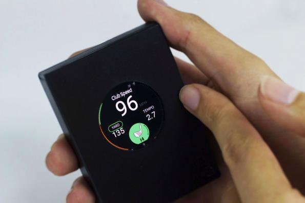
Truly is currently operating two production lines: the P1 and P2 lines, both 2.5-Gen and with a monthly capacity of 625K and 1.25M pcs (Truly counts its capacity as per 1" displays). Truly has set out to build two new production lines. The P3 line which is a 2.5-Gen line with a capacity of 3.13 million 1 panels monthly is almost ready and will start mass production by the end of the month.
UBI Research sees PECVD as the in-organic TFE equipment of choice for flexible OLED production
UBI Research says that as OLED makers are diverting all efforts into flexible OLED production, thin film encapsulation (TFE) is gaining in popularity. Between 2017 and 2021, TFE will be applied to about 70% of all OLED panels in production. The OLED encapsulation equipment market will generate $11 billion in sales.
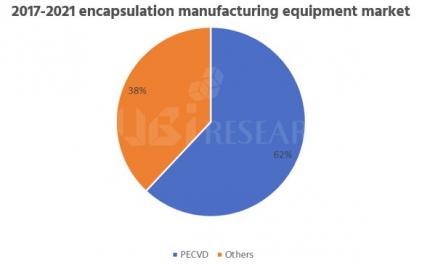
TFE encapsulation started out as a complex technology that required 11 layers and was slow and expensive. Recent advances allowed OLED makers to reduce the number of layers to just 3 and increase productivity and yields and so lower the production costs. Some film OLED makers opted for hybrid encapsulation (which uses a barrier film) but TFE seems to have become the technology of choice.
The US DoE awards five new OLED project grants
The US Department of Energy announced 11 new solid state lighting projects grants, out of which five are related to OLED technologies (the rest are for new LED technologies).
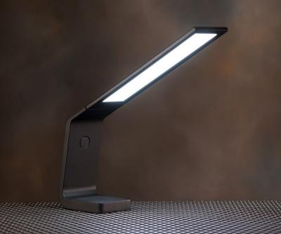
We already posted on two of these grants which were awarded to Pixelligent. In addition to Pixelligent, OLEDWorks were also awarded with two SBIR Phase 1 projects, one for an ultrathin, curved, high-efficiency OLED light engine that will reduce the cost OLED lighting and the second for the development of a novel substrate and encapsulation process.
Fraunhofer FEP develops a high-accuracy fingerprint sensor based on its bi-directional OLED microdisplays
The Fraunhofer FEP institute in Germany first unveiled its bi-directional OLED microdisplays in 2012 with the novel idea of embedding photo detectors between the OLED pixels. Since then the instituted demonstrated its second-generation microdisplay that supported a resolution of 800x600 (SVGA), up from VGA in the first generation prototypes.
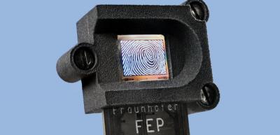
The Fraunhofer FEP now announced that it developed a new generation of these displays, that employ an extra-think encapsulation layer, which can turn these new displays into fingerprint sensors. The idea is that the OLED display illuminates the fingers and then the reflected light is used to detect and analyze the fingerprint with excellent accuracy.
Pagination
- Previous page
- Page 4
- Next page


