UK-based SmartKem develops a new class of flexible high-mobility OTFT display backplane technologies. The company provides customized solutions involving molecular synthesis, electronic prototyping and on-site technology transfer support.
As Smartkem is developing new backplane materials for OLEDs, ePaper and mini-LED devices, we discuss its technology and business with the company's CEO and chairman, Ian Jenks.
Q: Hello Ian, thank you for your time. Can you please first explain SmartKem’s OTFT stack?
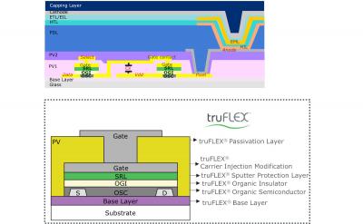
SmartKem has developed a complete OTFT stack trademarked truFlex(R) that consists of 6 layers Base Layer, Organic Semiconductor, Organic Insulator, Sputter Resistant Layer, Carrier Injection Modification and Passivation Layer that utilize a low mask count process, compatible with industry standard deposition, etching, slot die coating processes and has been used in applications ranging from flexible OLED and ePaper displays, X-Ray sensors, MiniLED backlights and others.
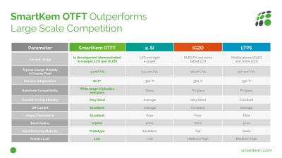
Q: What kind of performance can currently be achieved by your OTFT? How does it compare to LTPS and IGZO?
SmartKem’s OTFT solves a problem that's been plaguing the industry for over two decades, in that, we are able to offer a low temperature process on a flexible substrate at a lower cost than current technologies.
truFLEX uses a 80degC process vs a 300degC+ process for the competition; truFLEX as the name suggests is perfectly suitable for flexible devices which are quickly becoming reality in phones and tablets and laptops, it offers a 0.5mm bend radius vs a 2-5mm bend radius in other technologies; using existing manufacturing techniques and equipment, we are able to achieve the lowest cost product that is already ready for mass production.
Q: Does Smartkem offer its inks, in addition to the process technology to deposit them?
We offer both; we are able to supply mass production inks from our licensed partners as well as prototype inks from our own facility; in addition we are able to work with our customers to enable the design of the final product at their factory on their existing lines
Q: Smartkem says its OTFTs enable higher flexibility. What does that mean exactly for displays? How will OTFT displays be different then the current crop of flexible/foldable/rollable OLEDs?
We offer several advantages in our product to enable flexible displays in mass production, they include more rugged and robust materials, more flexible than what is out there, lighter, lower cost etc; the industry is currently using 2 to 5 mm bend radius as a standard, we are able to offer 0.5 mm bend radius, upto 10X better; most materials dent or break when subject to a ball drop test which is industry standard process to determine display ruggedness, we pass this test with flying colors. You can bend, roll, fold displays with our materials better than any traditional materials.
Q: We understand Smartkem currently mostly target miniLED backlights, when can we expect an OTFT backlight TFT for miniLED BLUs?
We have built samples of miniLED backlights using our substrate which has substantial advantages over the current method that uses FR4; we are aiming at true HDR performance by enabling Full Array Local Dimming (FALD) to allow LCD’s to compete effectively in the market by improving contrast, using materials that are thinner, lighter, versatile and much lower cost than IGZO or LTPS.
Mini LED backlights are also a precursor to the next generation of direct illumination microLED displays which will require an active matrix array to control an display of highdensity RGB microLEDS.
Q: Smarkem also targets the OLED and ePaper applications. Can you update on your status? What is your main value for the flexible OLED/ePaper?
OLED displays are the market leaders for a high quality user experience and are ideally suited to the stable current matrix arrays that we produce. If you want to deploy flexible OLED or ePaper, just like in the silicon world you need three things for mass deployment. You need the flexible raw materials, just like in silicon you need materials that are optimized for all the layers that make up a transistor circuit, you need EDA tools so designers can make and test virtual circuits and you need foundry services where parts can be made. Unlike the silicon world who had to make it up as they went along we have the benefit of following a well established industry business model. Materials, EDA tools, foundry services.
At SmartKem, we have both a long history of successfully developing materials and industry leading materials when it comes to performance; we have built the first set of EDA tools and enabled both prototype and mass production factories that can scale with the customer deployment.
Tomorrow we expect the best in class OLEDs to run on our material sets, we also expect to enable best in class color ePaper.
Thank Ian, good luck to both you and SmartKem!


