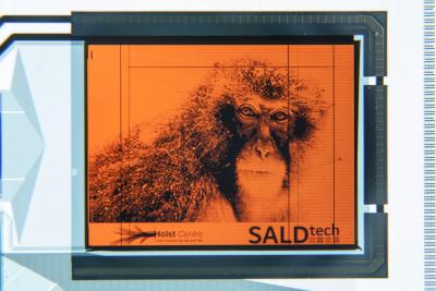
Researchers from the Holst Center has applied spatial atomic layer deposition (sALD) to create both the semiconductor and dielectric layer in a thin-film transistor (TFT) Oxide-TFT (IGZO) display backplane - for the first time ever.

The researchers created a 200 PPI QVGA OLED display prototype on a thin PEN foil. This shows how TFTs can be produced in a low temperature process (below 200 degrees Celsius) using sALD on a cheap transparent plastic foil. The TFTs achieved a mobility of 8 cm2/V2 with channel lengths down to 1 um.
The sALD equipment was developed by the Holst Center, and is being commercialized by the start-up SALDtech which was spun-off form the Holst. SALDtech current offers 1-Gen (320x250 mm) tools and is now developing production equipment.

