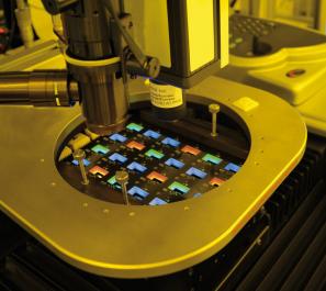
Researchers from the Fraunhofer FEP institute developed a new micro-patterning process using an electron beam to produce OLED microdisplays on silicon substrates. This could enable a new way to produce direct-emission OLED microdisplays, which will be more efficient and bright compared to the current ones that use color filters.

The electron beam patterning is performed after the encapsulation step - the beam goes through the encapsulation layer and can be used to modify the emission of the OLED materials. To create red, green, and blue pixels, an organic layer of the OLED itself is ablated by a thermal electron beam process.
Fraunhofer FEP researchers demonstrated electron beam patterning of OLED lighting panels two years ago. The researchers now aim to work with industry partners to co-develop the technology, integrate it into existing processes and eventually license it out for production.

