RiTDisplay starts to mass produce AMOLED displays on a-Si backplanes

There are reports that RiTdisplay started to mass produce 3.5" 320x480 AMOLEDs on a-Si backplanes, and the company was already contracted to provide the displays to several smartphone makers. a-Si backplane AMOLEDs will be cheaper and easier to produce than LTPS ones (which is the most common technology for AMOLEDs and next-gen LCDs such as Apple's Retina displays) as they can use existing a-Si equipment used to fabricate LCD displays.

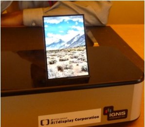
Canada's Ignis Innovation provided the compensation technology and driver IC (which is made by Himax). These are the same panels unveiled at SID last month. The actual backplane was developed with an undisclosed display-panel maker partner in Taiwan.

Read the full story Posted: Jun 02,2011

Nanomarkets: OLED material sales to reach $2 billion by 2016

Nanomarkets released a new report (The Market for OLED Materials 2011) in which they predict that OLED display and lighting material sales will exceed $2 billion in 2016. Mass market for OLED TV and OLED lighting will emerge in 2013 to 2015 which will boost the OLED material market.

Nanomarkets also believe that there will be more IP challenges and a trend towards "reverse engineering". Most OLED panels will use small molecules, but polymer OLEDs will begin to appear and will generate over $255 million by 2016 (i.e. around 12% of the total OLED marker).

Read the full story Posted: Jun 01,2011

TDK's transparent PMOLED - some technical details

Yesterday we posted that TDK started to mass produce transparent PMOLEDs, and now we have some technical updates. It turns out that TDK is not using transparent cathodes and anodes: only the anode is transparent, while the cathode is still made of metal. What they did is reduce the line width of the cathode so only a part of the pixel is covered. TDK calls this panel structure "thin-line electrode structure".

This is how they achieved 40% transmittance. This also explains why viewing this display from the back side is impossible (it is not clear - although parts are showing). TDK claims this is good because users will not want other people to view their phone display from the other side.

Read the full story Posted: Jun 01,2011

Mitsubishi installed a 6-meter OLED 'sphere' in Tokyo's Science Museum, uses smaller Diamond Vision panels

Update: Here's a nice video showing the Geo-Cosmos OLED globe in action

Mitsubishi Electric installed a new six-meter OLED 'globe' (called "Geo-Cosmos") at the National Museum of Emerging Science and Innovation in Tokyo, Japan. This is the world's first large-scale spherical OLED display and it will be unveiled on June 11. The globe will replace the existing LED globe and will show scenes of clouds and visions of the earth taken from a meteorological satellite.

The OLED Geo Globe

This is a Diamond Vision OLED - which means that it's made out of small PMOLED modules. In fact it uses 10,362 panels (!) - each 96x96mm in size - total resolution is more than 10 million pixels. Each module has 32x32 resolution - and it's made out of 4 smaller sub-modules (see below). Anyway it's news to us that Mitsubishi developed these smaller modules - previous modules were 384x384mm in size and 128x128 in resolution. Obviously this is useful to make curved or spherical displays.

Read the full story Posted: Jun 01,2011