Solution based OLEDs

The end of the OLED process monoculture - what will it mean for supply chain companies?

For most of OLED's commercial history, the industry operated as a near-monolith: virtually every panel maker deposited RGB organic materials through a Fine Metal Mask (FMM) on 6th-generation glass (or polyimide substrates with a glass carrier), while LG Display stood as the sole practitioner of its WRGB architecture for large-area OLED production.

In recent years, we have seen the emergence of new OLED architectures, processes and materials that signal the end of this technological uniformity. In this article, we examine the different technologies, speculate how the industry is changing and where it is headed - and understand the implications for supply chain companies. 

Read the full story Posted: Apr 01,2026

Researchers suggest a new four-step process to pattern solution-processable OLED emitter layers without UV radiation or etching

Researchers from Sogang University, the Ulsan National Institute, Hanyang University, and Yonsei University developed an indirect method for photopatterning of solution-processed OLED emitter layers (EML). The new method does not involve any direct exposure to UV radiation or harsh etching processes. 

The new process starts by forming a sacrificial photoresist (PR) pattern, followed by spin-coating of the EML film. The next step involves converting the EML film into a single-phase network (SPN) structure by crosslinking vinylbenzyl-group-appended hosts and dopants at a low temperature, and the final step is when the pre-formed PR pattern is stripped. 

Read the full story Posted: Jul 26,2025

Toray Research Center shows how OLED inspection and analysis enable the production of higher performance OLED panels

Toray Research Center (TRC) has launched a new open online webinar focused on OLED inspection and analysis technologies. TRC, who supplies technical analysis and support for R&D and manufacturing, invites you to attend the online lectures at no cost, to get a deeper understanding on OLED inspection and analysis, and how to achieve higher performance displays. The webinar recordings are accessible until February 15.

Toray Research Center TRC banner

The webinar include four presentations:

  • Identification of Trace Impurities Using High-Resolution Mass Spectrometry (Toward High-Quality OLED Panels)
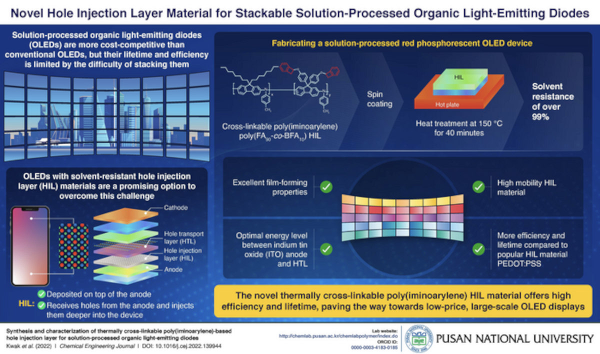
  • Analysis of Small Molecule OLED Layers in Solution Process and Vacuum Deposition Process
  • Moisture Diffusion Evaluation in Encapsulant
  • Analysis of QD sheet (Quantum Dot Enhancement Film)

The first presentation, titled Identification of Trace Impurities Using High-Resolution Mass Spectrometry (Toward High-Quality OLED Panels), details examples of possible degradation in OLED devices that lead to performance reduction. In this presentation, TRC discusses the role of analysis, the advantages of high mass resolution, different evaluation techniques and how it can help developers increase the performance of OLED displays.

Read the full story Posted: Feb 06,2024

Researchers developed a high performance, low-cost HIL material for solution-processed OLEDs

Researchers from Korea's Pusan National University have developed a new low-cost hole injection layer (HIL) material for solution-processed OLEDs, achieving higher efficiency and lifetime compared to the current state-of-the-art.

The new material is solvent-resistant (>99%) and thermally cross-linkable. The researchers used this material to create a solution-procssed red phosphorescent OLED device. The researchers placed the material between the ITO electrode and the HTL material, thus achieving photo-crosslinking of (poly-TPD) as HTL on top of crosslinked HIL. 

Read the full story Posted: Mar 16,2023

Is current OLED architecture obsolete? An interview with the head of Germany's Max Planck Institute

Researchers from Germany's Max Planck Institute, led by Prof. Paul W.M. Blom, are looking into single-layer OLED devices (in which a single emitting layer is sandwiched between two electrodes), with an aim to match their efficiencies to those of common multilayer OLED stacks, like the ones used in commercial OLED displays.

Current OLED architectures utilize multilayer stacks of materials, in order to increase the performance and lifetime of OLED devices. But according to the latest findings by Prof. Blom, equal efficiencies can indeed be met with single-layer TADF OLED emitters - and there's no fundamental reason or major benefits that arise from multilayer OLEDs.

Read the full story Posted: Feb 02,2023 - 2 comments

Samsung Display developed a 18.2" 350 nits ink-jet printed OLED panel

Samsung Display has developed a 18.2" 2560x1440 202 PPI inkjet-printed OLED display, that features the highest current efficiency of any inkjet-printed OLED, with the brightness at 350 cd/m2 (full white).

Samsung Display 18.2'' ink-jet printed OLED (SID DW 2020)

Samsung Display says that the high brightness was achieved by tuning the top-emission device structure with high performance soluble materials. The high pixel resolution was achieved by modulating the jetting waveform for ejecting ink drops and improving the drop placement accuracy by selecting the right ink formulations in terms of viscosities and surface energies.

Read the full story Posted: Aug 08,2020

Digitimes: AUO to build a 6-Gen OLED ink-jet printing line

Digitimes reports that AU Optronics has setup a 3.5-Gen test ink-jet OLED printing line, and the company now intends to start building a 6-Gen production line. AUO will start constructing the line before the end of 2019.

AUO's Chairman confirmed that the latest advances in printing materials and equipment are starting to make OLED printing viable for commercial use. AUO has not yet decided the schedule for volume production.

Read the full story Posted: May 02,2019

LG Chem acquires DuPont's soluble OLED IP and technologies

LG Chem has acquired DuPont's soluble OLED technologies and assets, in a deal estimated at $175 million. LG Chem will receive DuPont's entire soluble OLED IP (540 materials and process patents) and all of DuPont's related equipment and R&D facilities. The deal does not include any assets related to Dupont's evaporation OLED business.

LG Chem and DuPont soluble OLED technologies acquisition ceremony

LG Chem believes that the OLED industry is moving towards ink-jet printing of OLED panels based on soluble OLED materials and technologies - and it has now acquired key technologies in this area. DuPont has been developing related materials for over 20 years, has been collaborating with equipment makers (such as Kateeva) and display makers and has also developed its own nozzle-printing process.

Read the full story Posted: Apr 03,2019 - 3 comments