 The Fraunhofer Institute for Photonic Microsystems (Fraunhofer IPMS) is a research institute dealing with electronic, mechanical and optical components and their integration into devices and systems.
The Fraunhofer IPMS has been working on OLED since 2000, and in 2009 it launched a new department called COMEDD (the Center for Organics, Materials and Electronic Devices Dresden) to handle its OLED research and pilot fabrication. COMEDD was turned into an independent Fraunhofer Institute in 2012, later it became a business unit at Fraunhofer FEP, and in early 2024 it moved back into the IPMS.
The COMEDD researchers used to develop OLED lighting technologies, and OLED microdisplay technologies. Today most of the focus is into OLED microdisplays.
Maria-Reiche-Str. 2
01109 Dresden
Germany
Researchers at the Fraunhofer IPMS develop semi-transparent OLED microdisplays
Researchers from the Fraunhofer IPMS have developed a semi-transparent high resolution OLED microdisplay, that is significantly lighter than conventional combiner-based optical see-through near-to-eye systems. The specification of the display was not disclosed, but one can see it's a monochrome yellow panel.
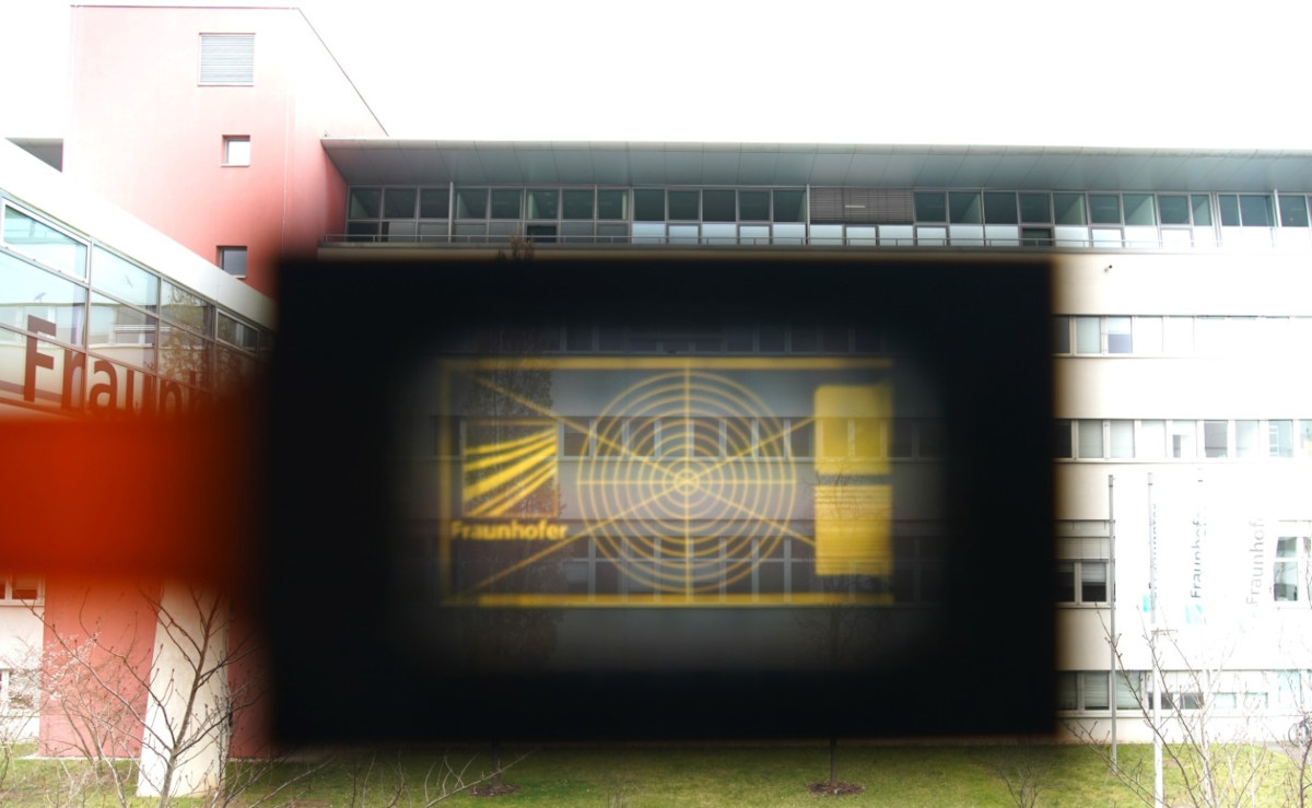
The Fraunhofer researchers developed a new semi-transparent OLED-on-silicon microdisplay technology, which enabled the new display. The technology is based on modern and advanced silicon CMOS processes, applied to silicon-on-insulator (SOI) wafers. The new wafer technology can be used to implement very thin circuitry layers. With the help of a specific IC design and an appropriate transfer-to-glass process flow, the transparent OLEDs were enabled.
The Fraunhofer FEP showcases its latest OLED microdisplays at Display Week 2023
During Display Week 2023, the institute demonstrated its latest displays, including the world's highest-density OLED microdisplays, reaching a PPI of 10,000 with a pixel size of only 2.5 um.
Fraunhofer's 10,000 PPI display was e a 0.18" 1440x1080 (monochrome) panel, produced on 300 mm wafers, using a 28 nm backplane process. The Fraunhofer also showcases ultra low-power microdisplays, and more technologies.
The Fraunhofer FEP developed the world's highest density OLED microdisplay, reaching 10,000 PPI
The Fraunhofer FEP research institute announced that it has developed the world's highest-density OLED microdisplays, reaching a PPI of 10,000 with a pixel size of only 2.5 um. The Fraunhofer will demonstrate a 0.18" 1440x1080 (monochrome) OLED microdisplay next week at Display Week 2023.
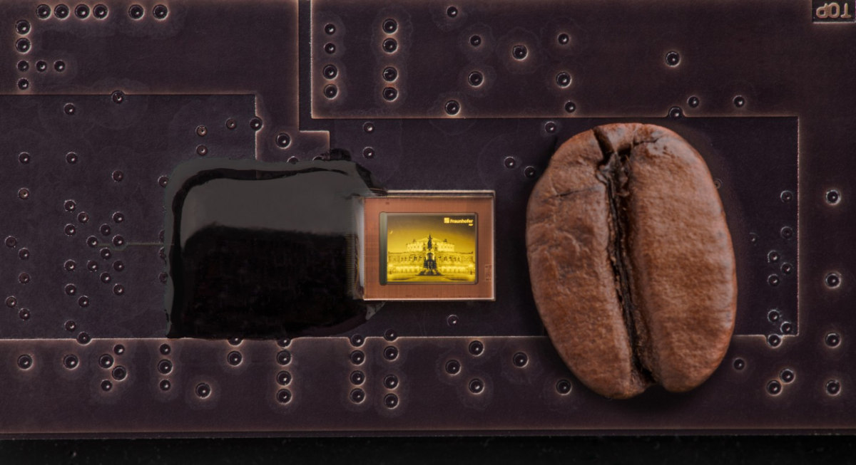
The new microdisplays were produced on 300 mm wafers, using a 28 nm backplane process. The Fraunhofer explains that most OLED microdisplays to date are produced on 200 mm wafers, using CMOS processes ranging from 90-250 nm. The institutes new technologies enables the the performance increase in OLED display processing.
The Fraunhofer Institute develops ultra-low power OLED microdisplays
The Fraunhofer FEP, in collaboration with GlobalFoundries Dresden Module One and digades, developed an ultra-low power color OLED microdisplay. The researchers at the Fraunhofer say that this display consumes the least power compared to all available microdisplays.
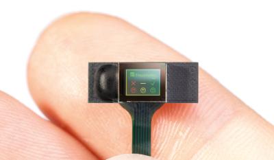
The new microdisplay was developed as part of the Backplane project, funded by the German government (SWMA grant number100392259). The researchers presented a prototype display that features two primary colors and a QVGA (320x240) resolution. The display is based on the Fraunhofer's existing OLED-on-silicon technology, which up until now was used to create monochrome microdisplays.
OLED webinar to introduce OLED lighting manufacturing and R2R production
An AILU (Association of Industrial Laser Users) webinar, scheduled for September 15, will introduce the basics of OLED lighting, discuss the choice for the right substrate and encapsulation material as well as the current status of roll-to-roll processing. The webinar is sponsored by 3D Micromac, the industry leader in laser micromachining and roll-to-roll laser systems.
The webinar will also show results from the EU-funded LAOLA project, which is a collaboration between German and Japanese companies and research institutes. The LAOLA project, led by the Fraunhofer FEP, develops the use of ultra-thin flexible glass as a substrate and encapsulation material in roll-to-roll technology for this purpose.
The Fraunhofer FEP shows its latest OLED technologies, creates a new virtual tour of its facilities
The Fraunhofer FEP Institute published this nice video that shows its latest technology innovations, including its OLED (regular and bi-directional) microdisplays, its new AR/VR optics, flexible OLED lighting panels, its Monarch flexible and transparent OLED panels, sensor and coating technologies and more.
The Fraunhofer FEP also created and published a new virtual tour of its facilities, where you can have a look inside the labs and flexible organic electronics R&D clearnroom.
Notion Systems, MBraun and the Fraunhofer IAP develop a novel display industrial production process based on inkjet printing
Notion Systems, MBraun and the Fraunhofer Institute for Applied Polymer Research (Fraunhofer IAP) are co-developing new inkjet production technologies, aimed for the display market - specifically for OLED, QD and microdisplays.
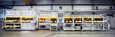
The three partners are combining their respective competencies to present themselves together as a partnership supplier off all-in-one solutions. The Fraunhofer IAP is developing custom-made processes for display manufacturing with tailor-made inks. To achieve an industrial-scale best-in-class process solution, the parties are looking into all major pre-and post-processing steps, the substrate and the production equipment such as the inkjet print head.
SEL developed a flexible OLED with embedded photo detectors between the OLED pixels
Researchers from Semiconductor Energy Laboratory (SEL) developed flexible OLED displays that incorporate organic image sensors inside the OLED pixels using side-by-side patterning. The sensors can be used as cameras for applications such as fingerprint sensing - which will work on the entire display.
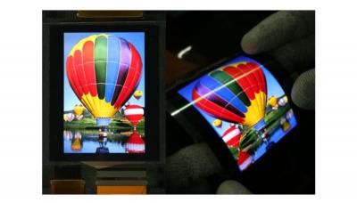
SEL presented two prototypes, one a 3.07" 360x540 (212 PPI) display and the second is a 8" one with a higher pixel density of 302 PPI. SEL says that the fingerprint recognition works even when the display is bent.
The Fraunhofer suggests using bidirectional OLEDs to create smart antibacterial surfaces
The Fraunhofer first demonstrated its bi-directional OLED microdisplays in 2009 - these display use photodetectors embedded between the OLED pixels to enable unique applications such as eye-tracking and more.
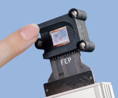
The Fraunhofer now suggests a new use for such displays. The BiClean project looked into the possibility of embedding bi-directional OLED microdisplays in solar panels or pipes, to detect contamination in early stages. The display project light at different colors, and the photodetectors can sense the surface status in real time - and so it is possible to know whether it is necessary to clean the surface.
The Fraunhofer FEP Monarch flexible transparent OLED lighting kit - hands on review
In 2018 the Fraunhofer FEP institute announced it is starting to offer a design kit that includes several flexible and transparent OLED lighting panels. The Monarch Kit includes several colored butterflies samples, and the researchers were kind enough to send us one such kit for a short review.
So first of all, these OLEDs look beautiful. They shine a beautiful uniform colored light and are very nicely done. There's not much functionality, but it shows the potential of flexible OLED lighting quite nicely.

