Vacuum evaporation

Researchers use intermittent vacuum deposition to increase OLED device performance

Researchers from Japan's Chiba University developed a new method to deposit thin OLED layers that achieves controllable molecular arrangement - that can be used to increase the efficiency and lifetime of OLED devices.

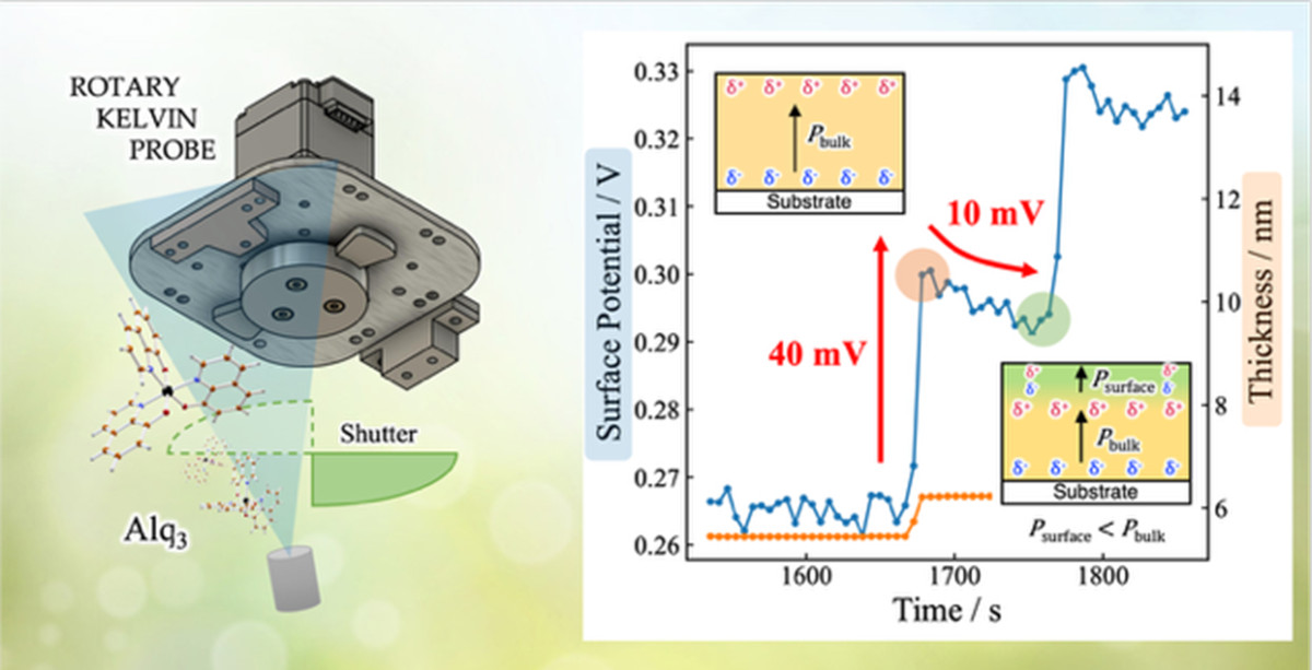
The method, called intermittent deposition, uses pauses in deposition and changes in deposition conditions to invert the orientation of the organic molecules, thus achieving high control over the resulting films. The researchers built on a tool called Rotary Kelvin Probe (RKP) that is used to measure the surface potential during and after the deposition in real-time. The new approach of intermittent deposition created a relaxed and stable surface layer with controllable polarization. 

Read the full story Posted: Jan 18,2024

UDC announces new narrow-spectrum PHOLED materials, reports advances in OVJP deposition technology

Universal Display announced that it will detail advances in its latest PHOLED materials at Display Week 2023. The company's latest red, green, and blue PHOLED materials offer a narrow emission spectrum, which increases the efficiency of OLED devices, in addition to enhancing the color gamut.

UDC PHOLED materials photo (2017)
UDC also unveil a new OVJP system printed on a 200mm x 500mm Corning Astra Glass substrate. UDC will also showcase the first-ever fully printed seven-layer (HIL/HTL/EBL/EML/HBL/ETL/EIL), 80 PPI, green commercial-level PHOLED device fabricated by its R&D OVJP system that has comparable device performance with vacuum thermal evaporation (VTE). 

Read the full story Posted: May 22,2023

Is current OLED architecture obsolete? An interview with the head of Germany's Max Planck Institute

Researchers from Germany's Max Planck Institute, led by Prof. Paul W.M. Blom, are looking into single-layer OLED devices (in which a single emitting layer is sandwiched between two electrodes), with an aim to match their efficiencies to those of common multilayer OLED stacks, like the ones used in commercial OLED displays.

Current OLED architectures utilize multilayer stacks of materials, in order to increase the performance and lifetime of OLED devices. But according to the latest findings by Prof. Blom, equal efficiencies can indeed be met with single-layer TADF OLED emitters - and there's no fundamental reason or major benefits that arise from multilayer OLEDs.

Read the full story Posted: Feb 02,2023

A report suggests that Samsung Display is interested in JDI's eLEAP OLED deposition technology

A few months ago, Japan Display (JDI) announced that it has developed a "historic breakthrough in display technology" - a new OLED deposition process which they refer to as eLEAP, that is said to be cost effective and can be used to create freeform OLEDs that are brighter, more efficient, and longer lasting compared to OLEDs produced using mask evaporation (FMM).

JDI eLEAP aperture ratio image

According to a new report from Korea, Samsung Display is interested in JDI's new technique. Interestingly the report shows conflicting views within SDC - some are interested in adopting this new technology, especially at SDC's upcoming 8-Gen IT OLED production line, while others are more interested in preventing SDC's competitors (JDI, or others?) from using it, perhaps by pressuring OLED equipment makers to not offer needed equipment to JDI.


Read the full story Posted: Sep 21,2022

Samsung Display developed a 18.2" 350 nits ink-jet printed OLED panel

Samsung Display has developed a 18.2" 2560x1440 202 PPI inkjet-printed OLED display, that features the highest current efficiency of any inkjet-printed OLED, with the brightness at 350 cd/m2 (full white).

Samsung Display 18.2'' ink-jet printed OLED (SID DW 2020)

Samsung Display says that the high brightness was achieved by tuning the top-emission device structure with high performance soluble materials. The high pixel resolution was achieved by modulating the jetting waveform for ejecting ink drops and improving the drop placement accuracy by selecting the right ink formulations in terms of viscosities and surface energies.

Read the full story Posted: Aug 08,2020

UDC establishes a subsidiary to advance OVJP commercialization

Universal Display established a new subsidiary, called OVJP Corporation, that will advance the commercialization of UDC's OVJP OLED TV manufacturing technology.

OVJP stands for Organic Vapor Jet Printing, and the basic idea is to use a gas-stream based process that resembles ink-jet printing but one that uses evaporation OLED materials. In an OVJP process, the OLED materials are evaporated into a carrier gas that delivers them to a jet engine for direct printing of patterned OLED layers.

Read the full story Posted: Jul 15,2020

DSCC - OLED material sales will grow from $951 million in 2019 to $2.69 billion in 2024

DSCC updated its OLED material market estimates, saying that AMOLED stack material sales will grow from $951 million in 2019 to $2.69 billion in 2024 - a CAGR of 23%. These new estimates take into account DSCC's reduced input area forecast due to the slowdown in demand cased by the Covid-19 pandemic.

AMOLED material revenues (2019-2024, DSCC)

DSCC says that incremental improvements in material utilization and price reductions, material costs per square meters will decline in the future. The unyielded cost of producing a square meter of a WOLED TV panel will decline from $95.21 in 2019 to $56.11 in 2024.

Read the full story Posted: May 08,2020

The Fraunhofer FEP Monarch flexible transparent OLED lighting kit - hands on review

In 2018 the Fraunhofer FEP institute announced it is starting to offer a design kit that includes several flexible and transparent OLED lighting panels. The Monarch Kit includes several colored butterflies samples, and the researchers were kind enough to send us one such kit for a short review.

So first of all, these OLEDs look beautiful. They shine a beautiful uniform colored light and are very nicely done. There's not much functionality, but it shows the potential of flexible OLED lighting quite nicely.

Read the full story Posted: Oct 14,2019

The Korea government to establish a $470 million OLED R&D center

The South Korean government announced a seven-year project to establish an OLED R&D and manufacturing facility in Cheonan, South Chungcheong Province.

The Korean government will spend 528 billion Won (around $468 million USD), it's largest ever R&D project, to build the R&D center and manufacturing facility, which will include 61 manufacturing and production systems, including several OLED evaporation systems. The R&D facility will conduct over 66 planed projects, focusing on technologies such as flexible OLED encapsulation, cost-cutting methods, next-generation displays and more.

Read the full story Posted: Oct 17,2018

OLEDON developed a vertical-plane source deposition technology suitable for ultra-large substrates

Korea-based OLEDON announced that it has developed a vertical-plane source deposition technology that can be used to produce both small-area and large-area OLED panels. The company is now adapting this technology for ultra-large substrates - up to 12-Gen (3300x4000 mm) in size.

OLEDON OLED TV vertical plane source evaporator

OLEDON says that currently-used inline evaporation processes lower the yields for large-area production due to FMM sagging and difficult control of the multiple sources. The company's vertical plane source deposition may prove to be a viable alternative.

Read the full story Posted: Oct 03,2018