Yesterday a Taiwanese web site reported that Applied Materials is planning to setup a flat-panel R&D center in Southern Taiwan Science Park. The new center will focus on 8.5-Gen LCD production and OLED technologies. Applied hopes to assist AU Optronics and Innolux with their OLED projects. The investment in the center is expected to exceed NT$5 billion (over $170 million USD).
A few hours later, Digitimes posted that sources from Applied Materials denied these rumors - saying that the company has no such plans. Applied does have a manufacturing center in Taiwan that will continue providing solutions largely for Taiwan-based customers.
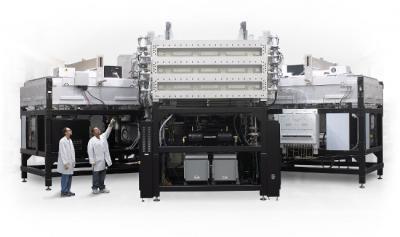
In November 2012 Applied Materials announced two new film deposition systems, used to make high definition televisions and high-resolution mobile device displays - both OLEDs and LCDs. The AKT-PX-PECVD is used for LTPS deposition on large glass substrates (sized from 1.6 m2 to 5.7 m2) while the AKT-PiVoT PVD system is used to deposit metal oxide-based TFTs (IGZO in particular).