 Universal Display Corporation (UDC) is one of the most known OLED company, involved with OLED IP, OLED phopshorescent materials, innovations on flexible OLEDs, production processes and more. As the most prominent public OLED company, the company is interesting to many investors and analysts.
Last year UDC hired Darice Liu to handle communications and investor relations. Darice was kind enough to answer a few questions I had regarding UDC's technology and business. These are interesting times for UDC as the OLED market is growing quickly, OLED TVs and flexible OLEDs are finally appearing on the market, but on the other hand the company is being faced with patent litigation and criticism from some investors (whom I shall not name).
Q: Hello Darice. Thanks for this interview! Your recent quarterly results were excellent... well done. Do you expect UDC's revenue to continue "tracking" the OLED revenue market?
Thank you. We were pleased to report another excellent quarter of profitability in our third consecutive profitable year. Looking back, in 2013 we achieved key milestones that reinforced our foundation for future growth. Our material sales more than doubled year over year. This was driven not only by the OLED market, as manufacturers scaled up production as well as developed new products, but also from the commercial adoption of our green UniversalPHOLED emitters and green hosts.
The OLED industry is clearly developing into an expanding growth market with increasing investment plans and growing product roadmaps. Across the company, we are building momentum for continued growth. That includes advancing our expertise for new materials and technology. We believe that our proprietary UniversalPHOLED materials are a critical element in helping to reduce display power consumption. Looking at 2014 and beyond, we are excited for the promising growth that lies ahead of us.
Q: Some articles online claim that your deal with Samsung includes a clause that says the agreement can be nullified if some patents are revoked (so called termination rights). Is this true?
That is 100% incorrect. You can refer to the agreements we filed with the SEC for more color.
At UDC, we are committed to increasing the value of and defending our intellectual property portfolio by building upon and around our core fundamental phosphorescent patent families. We have a growing portfolio of more than 3,300 issued and pending OLED device, architecture, and material patents worldwide. This comprehensive global IP framework is designed not only to fortify Universal Display’s licensing and materials business model, but to help ensure that the trajectory of our future will not be defined by any one patent or decision, favorable or unfavorable.
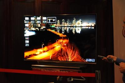
Q: Last year, during you ASM, you exhibited LG's 55" OLED TV. It was assumed before that LG is using PHOLED materials in their TV. Are you able to detail more about which of your materials and technologies LG is using in those TVs?
LG Display is a valued customer, whom we have worked with for years. We expect to play a key role in the growth of the OLED TV market.
Q: Can you also give some details as to what materials are used in SDC and LGD's flexible OLEDs? Are green PHOLEDs used in those panels?
Both SDC and LGD are valued long-term customers. The OLED materials used in flexible displays are the same materials that are used in glass-based products. We cannot comment on specific products though.
Q: During the ASM, you also mentioned the OVJP deposition technology. Can you update us on your OVJP?
Our patented organic vapor jet printing (OVJP) process is one of the areas that we feel is important for the future growth of the OLED industry. It combines the high-performance of small molecule materials, that are typically deposited using VTE, with the process efficiency of a direct printing process like ink-jet printing (IJP). This is achieved by flowing an organic vapor through a microscopic nozzle to form a highly collimated gas beam. As with IJP, this beam is then directed to print fine-featured organic patterns at very rapid rates. As such, OVJP offers a high-resolution printing capability with very high material utilization. It may also offer higher manufacturing cycle time and throughput than IJP because ink-jet well fabrication and a post-printing anneal step are not required. While the potential is tremendous, work remains. Stay tuned!
Q: Now that Samsung is adopting green PHOLEDs, OLEDs are more or less similar to the best LCDs in terms of power consumption. How do you see the next OLED efficiency breakthrough? Will that be from a blue PHOLED or some other technologies?
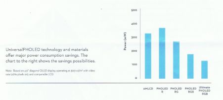
We believe that our proprietary UniversalPHOLED materials are a critical element to enable energy efficiency, reduce requirements for heat dissipation components, increase lifetime and lower product costs. We have been building on the success of our red phosphorescent OLED (PHOLED) emitters with the recent commercial adoption of our green PHOLED emitters. We believe that adding green where red PHOLEDs are already used creates more value. We estimate that our green PHOLEDs can improve power efficiency by approximately 25 percent in an OLED display.
The introduction and commercialization of green furthers our goal of providing manufacturers with an all PHOLED emissive system. We continue to develop new materials that will not only achieve record-breaking efficiency, but meet the needs of manufacturers and the devices of both today and tomorrow.
Q: Speaking of blue PHOLEDs, you mentioned before that the Fujifilm patent portfolio may help you to develop a commercial blue. I understand you're currently focused on entire-stack solutions, and not just a new emitter. Any advances you can report on that front? Is it likely that a dark-blue PHOLED will become commercial in the next year or two?
We continue to make progress with our blue PHOLED materials. We have taken the technology from a stage where some believed that it might not be possible to where we have demonstrated each of the key metrics: excellent luminous efficiency, blue saturation, and long lifetime. We currently have a light blue PHOLED emitter with CIE color coordinates of (0.18, 0.42) with a luminous efficiency of 50 candelas per ampere (cd/A) and 20,000 hours of operating lifetime to half-life at 1000 candelas per square meter (cd/m2).
We continue to work diligently to develop blue PHOLEDs, including utilizing some of the Fujifilm patents we acquired, that will meet commercial requirements. When we achieve meaningful advances, we will announce them.
Q: A few years ago you suggested an RGBB architecture to adopt a light blue PHOLED sub-pixel. Has there been any interest in this design? Is it still being investigated and developed?
We continue to develop materials to suit manufacturers’ needs, and we’re testing a range of PHOLED systems with our manufacturing partners. The RGBB architecture has demonstrated the potential to meet manufacturers’ needs, and it could be a solution to meet the goal of an all-PHOLED materials system sooner than a standard RGB structure.
Q: One of the key technologies that may enable flexible OLED production is the encapsulation. When do you expect to be able to scale-up your UniversalBarrier tech for larger substrates which may enable mass production? Will you team-up with an OLED manufacturing equipment maker to develop this?
Encapsulation is another key future technology that can be extremely beneficial in helping to support continued industry growth, especially for plastic and other flexible substrate based products. As you are aware, thin-film environmental barriers are required for OLED displays and lighting as well as flexible solar cells and transistor backplanes.
We have developed a novel, single-layer barrier technology for the cost-effective packaging of thin-film devices and plastic substrate systems. Our proprietary, patented encapsulation approach uses a single, hybrid layer that combines the impermeability of one component with the toughness of the second component to create an effective barrier. This barrier film offers excellent performance for application to both plastic substrates as well as directly onto OLED and other thin film devices. While the technology is still in the early stages, the process has demonstrated strong potential. Stay tuned!
Q: The OLED Lighting technology is advancing rapidly, but mass production is still not here. You recently signed a collaboration & supply agreement with Philips. How do you see this market evolving? Do you share analyst forecasts saying that the market will emerge at around 2015-2016, or is that too soon? Can you estimate when will OLED lighting revenues start to get meaningful for UDC?
Energy-efficient white OLEDs hold a great deal of promise for creating never-before-seen products with innovative form factors, including curved, transparent and flexible lighting. A lot of the focus early on in OLED development was on displays, but the development in lighting is picking up speed. In fact, just recently manufacturers announced progress in OLED lighting performance using phosphorescent OLEDs as well as new manufacturing capacity.
The products and prototypes from global lighting manufacturers are creating quite a bit of buzz in the industry, and we’re working with them to continue to develop our materials and technologies that fit the direction of OLED lighting players. We’re excited about our recent agreement with global lighting manufacturer, Phillips, and chemical conglomerate, Kaneka Corporation, and we’re also working with several other manufacturers to advance this technology. It is difficult to predict how rapidly this industry will grow. However, all the activity is very encouraging.
Q: Some people believe that soluble OLEDs and Inkjet printing is the best process for low-cost large-area OLEDs (and it seems that the ink-jet technologies are maturing quickly). Do you subscribe to that view as well? How are your soluble OLEDs advancing?
Soluble OLEDs and inkjet printing offer alternative manufacturing opportunities, and we continue to develop our UniversalP2OLED materials to meet the potential demand for these manufacturing processes. UniversalP2OLED printable, phosphorescent OLED materials and technology are under development to combine the high efficiency of our UniversalPHOLED technology with potential low-cost solution processing techniques. If these techniques can be commercialized, we will be ready with our UniversalP2OLED materials!
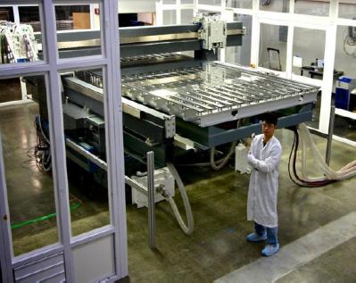 Kateeva 8-gen OLED inkjet system
Thanks again Darice! I wish both you and UDC the best of luck...
Disclosure: The author of this articles (the questions bit, anyway) owns some shares in UDC