OLED is an emerging display and lighting technology that enables beautiful and efficient displays and lighting panels. Thin OLEDs are already being used in many mobile devices and TVs. Polymer-OLEDs (or PLEDs, also used to be called P-OLEDs) are OLED devices made from polymer (large-molecules) materials.

PLEDs vs SM-OLEDs
Basically you can make OLEDs from two kinds of materials: small-molecule (SM-OLED) or large-molecules, or polymers. Virtually all OLED displays on the market toady are using Small Molecules, and are produced using evaporation processes.
PLED (P-OLED) materials do not perform as good as SM-OLEDs in terms of lifetime and efficiency, but are easily soluble and so can be easily adapted for printing and other solution-based processes. In the past some believed that the soluble nature of PLEDs mean that these materials will be the future of OLED displays, but that has not been the case yet. There has been great progress in evaporation processes and materials - and also in soluble SM-OLEDs.
CDT / Sumitomo
UK-based Cambridge Display Technology (CDT) is the company that holds the basic patents for PLED technologies. The company licensed its technology to several companies, including Philips, Seiko Epson, Osram, Dupont and Delta Optoelectronics, but it does not seem as it anyone is pursuing PLEDs at the moment besides Sumitomo Chemicals (which owns CDT).
Sumitomo and CDT are still developing PLED materials and panels. Sumitomo is providing emitter materials for JOLED (who started low volume production of printed OLED monitor panels in December 2017, see below) and is hopefully gearing up to start mass production of its own OLED lighting panels.
JOLED's PLED
JOLED (Japan OLED) was established in August 2014 by Japan Display, Sony and Panasonic with an aim to become an OLED medium display (10-30 inch) producer, mostly targeting monitors and commercial applications. JOLED is using a printing process which should result in lower cost production (but of lower performance displays) compared to evaporation printing.

JOLED is using PLED materials produced by Sumitomo (see above). The company started commercial low-volume production of its 21.6" 4K OLED panels towards the end of 2017 at the company's pilot 4.5-Gen line. In 2021 JOLED started mass producing PLED displays at its 5.5-Gen line in Nomi City.
Panasonic's 2013 56" OLED TV prototypes
In January 2013 Panasonic unveiled a 56" 4K (3840x2160) OLED TV panel prototype that was produced using an all-printing method and PLED materials. Panasonic says that all the organic materials were deposited using ink-jet printing. The panel's TFT substrate was supplied by Sony (and actually made by AUO. It's an Oxide-TFT panel) as part of the two companies collaboration. The lifetime and efficiency of this TV was not disclosed.

In December 2013 Sony and Panasonic announced that they are canceling the OLED TV JV. Panasonic is now producing OLED TVs - but these use WRGB OLED panels produced by LG Display.
P-OLED (PLED) vs pOLED
P-OLEDs, or PLEDs, are a class of OLED materials. Somewhat confusingly, LG Display is branding its mobile flexible AMOLED displays as pOLEDs (plastic OLEDs). For more information on LGD's pOLEDs, click here.
Further reading
The latest PLED news:
Panasonic's OLED program is progressing fast, will launch 56" UHD OLEDs in Q4 2013?
According to the OLED Association, Panasonic said that they are progressing fast enough to launch the 55" (probably 56") UHD OLED TV in Q4 2013. Panasonic will start mass production in its Himeji Pilot Gen-5.5 line (which means initial production will be very limited). If this report is true it means a real acceleration as Panasonic previously said they will only be ready in 2015 (although you may say that the current Himeji line will not be real mass production in any case).
 Panasonic OLED TV prototype, IFA 2013
Panasonic's OLED TV panel, unveiled in January 2013, is produced using ink-jet printing and uses an RGB subpixel matrix (direct-emission). Panasonic is using Sumitomo's PLED materials, and AUO's oxide-TFT Substrates. The company is collaborating with Sony on OLED technologies.


New technology may lead to true white emitting OLEDs based on platinum-doped polymers
Researchers from the University of Utah developed a new polymer light emitting device that can be tuned to emit light of different colors, including white (without the need to mix several emitters). The new material is a polymer molecule doped with platinum. The same material can also be used to develop efficient OPVs or Spintronics-based memory devices.
The device currently being developed at Utah isn't an OLEDs as it only emits light when stimulated by other light (such as a laser) and not when simulated by an electrical current. But the researchers say that a white OLED based on this technology is possible and predict that it will be developed within two years. The current device isn't actually white, it emits colored color (more on this below) and they say it will take about one year till they manage to develop a white Pt-1 device.
Utah professor explains the science behind the Spin-OLED device
In 2012 we posted about a the Spin-OLED, a new spin-polarized polymer efficient OLED device developed at the University of Utah and the Israeli Technion. Now Professor Z. Valy Vardeny from Utah gave a talk (titled "Spin Effects in Organic Optoelectronic Devices") describing the Spin-OLED in more details:
Professor Vardeny also gives an introduction to organic Spintronics and introduces the hybrid organic/inorganic spintronics device and explains how OPV can be enhanced by spin 1/2 radical additives.
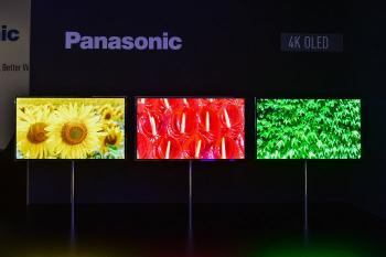
Panasonic shows OLED TV and lighting prototypes at IFA 2013
As promised, Panasonic showed 56" 4K (3840x2160) OLED TV panel at the IFA 2013 exhibition. The company had several prototypes on display, and I believe these are the same panels as the ones Panasonic unveiled at CES 2013 in January 2013.
Panasonic panels are made using an "all-printing" method, and Sumitomo Chemical revealed that these prototypes use the company's PLED materials. Panasonic's panel uses a substrate (probably Oxide-TFT) provided by Sony (which are actually made by AU Optronics) - as part of the two companies collaboration. According to the latest reports, they only plan to start OLED production at around 2015.
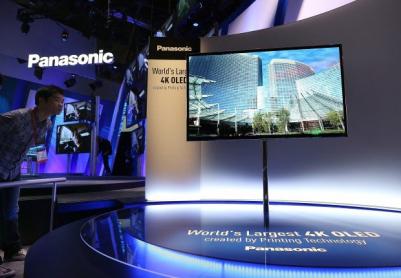
Panasonic's 4K OLED at IFA 2013
Some web sites are reporting that Panasonic is set to unveil a 20" 4K OLED tablet at the IFA 2013 event next week. Those sites are relying on auto-translated Japanese text. But in fact the company will not show such a tablet. In an English PR, Panasonic says they will show a 4K 20" tablet and a 4K OLED panel prototype - those are two different devices.

I'm guessing Panasonic's 4K OLED panel will be the same 56" 4K (3840x2160) OLED TV panel shown at CES 2013. This panel was made using an "all-printing" method. Sumitomo Chemical revealed that this TV prototype used the company's PLED materials. Panasonic's panel uses a substrate (probably Oxide-TFT) provided by Sony (which are actually made by AU Optronics) - as part of the two companies collaboration.
Philips, Merck and Audi developed 3D OLED prototypes for the Audi TT
Audi, Philips, Automotive Lighting, Merck and the University of Cologne successfully concluded an OLED research project (called OLED 3D), and developed the world's first large-area 3D OLED car rear lighting panels and installed a prototype on an Audi TT.

A 3D OLED means that the OLEDs have a curved surface - not just in one direction. These are glass based panels. It's not flexible glass (like Corning's Willow glass), it's the regular glass Philips are using in their regular OLEDs, but curved. The material used (made by Merck) are soluble, and the production process is described as "web printing" by Philips (I'm not sure what is meant by that).
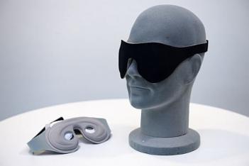
Researchers develop OLED-based "sleep mask" to treat sight loss noninvasively
Researchers from Northumbria University and PolyPhotonix developed a new OLED-based "sleep mask" that can be used to treat sight loss noninvasively. The researchers say that this new device is the world's first noninvasive primary-care treatment for diabetic retinopathy and age-related macular degeneration (AMD).
The researchers are already doing extensive clinical trials (at the home). They say that if this proves useful, it will be much cheaper than current treatments (and it's also non-invasive).
Sumitomo developed a new PLED inkjet printing technology
Sumitomo Chemical announced it has developed a new PLED inkjet-printing technology that achieves 423 PPI on glass substrates sized 370x470 mm. We don't have more information about Sumitomo's new production process, but apparently it isn't ready for commercialization yet as the company says they will "continue to improve the performance and process of PLED materials".
 Panasonic printed P-OLED 56-inch OLED prototype
Panasonic used Sumitomo's PLED materials in their 56" 4K2K printed OLED TV prototype shown at CES 2013. Panasonic and Sumitomo has been collaborating on OLED TVs since 2009. The companies hope that ink-jet printing will enable them to lower the production costs of OLED panels compared to evaporation based production. Panasonic aims to launch their first OLED TVs in 2015. The company is collaborating with Sony, and may setup a production-JV together (although if this happens, it's not clear which production technology will be used).
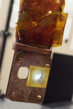
Sumitomo shows flexible, printed, structured PLEDs, will bring them to market by early 2015
Sumitomo Chemical unveiled new flexible PLED lighting panels. These structured panels (they have a patterned printed on them) are produced in an ink-jet printed process. Sumitomo showed several lamp prototypes, including the one shown below:
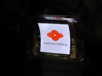
Sumitomo plans to start volume production of such panels by March 2015 (fiscal year 2014) - using both ink-jet and roll-to-roll processes. They still need to extend the lifetime of their panels, improve the luminance performance and improve their production yield rates.
CPI posts some updates on their OLED developments
The UK's Centre for Process Innovation (CPI) posted some updates on their OLED program. They have recently produced defect free OLED lighting samples. They managed to produce panels that has large (over 250 cm2) emissive areas (they are producing these panels on 8" substrates and so could exceed 160x160 mm panels).

The CPI developed two kinds of panels - the first uses small molecule materials and the second uses full solution-processable PLED materials. They have also produced samples that use a hybrid structure with a PEDOT layer (deposited using a slot die process) with an evaporative emissive layer (that has better efficiency and performance compared to the PLEDs). The 154x154 mm example shown above is the hybrid structure.