This is a sponsored article by Nanomatch
Recent applications of the Nanomatch Toolkit to improve OLEDs:
- Charge carrier mobility
- Charge screening in OLED materials
- Doping
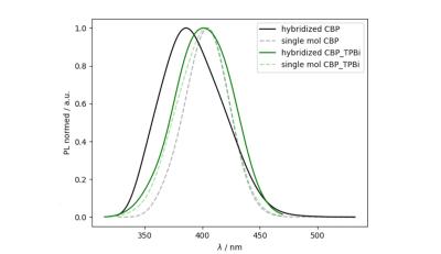
- Excited states in molecular thin films
Attend our talk at SID Display Week (Session 28 on May 11 2022, 10:40 AM) for further information.
Read more:
Charge carrier mobility
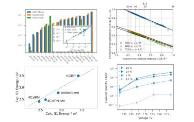
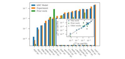
Tuning charge transport properties is a crucial step towards balanced OLED devices. Especially in mixed systems, it is challenging to predict conductivity or charge carrier mobility to fine-tune material combinations and layer setup. Here we illustrate how our software can predict charge carrier mobility for a set of diverse organic materials.
Charge screening in OLED materials
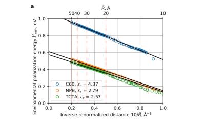
Polarization in organic semiconductor materials lead to modified properties of organic molecules embedded in thin films, compared to their properties in vacuum, such as ionization potentials or electron affinities. This renders their accurate prediction challenging even for the most experienced chemists. In this study we present a method to compute ionization potentials and dielectric permittivity for organic molecules.
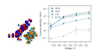
Doped injection layers are a common technique to overcome injection layers between electrodes and organic layers, and their optimization is highly critical for efficient OLED devices. These studies applies our software to investigate the impact of material and layer properties on injection barrier and device conductivity, to enable rational design of novel compounds for doped injection layers.
Read the full use cases here and here.
Excited states in molecular thin films
Excited states in emission layers depend on the interplay of excited state properties of emitter and host materials. This imposes a challenge on aligning multiple emitter materials in complex emission systems.
1) We observe that aggregation of molecules in the thin film leads to hybridization of excited states that can induce a strong shift of the excitation spectra.
2) Further we analyze the impact of matrix induced conformational changes of molecules in thin films on excited states and illustrate the role of electrostratic screening effects.
Why Nanomatch?
R&D of OLEDs is mainly driven by experience and chemical intuition, therefore strongly relies on trial&error which results in many development cycles and long time-to-market.
While there is a fundamental understanding of molecular properties of materials in form of isolated molecules, the complex interplay of material properties and microscopic processes in OLEDs renders it close to impossible to systematically predict the response of device properties such as efficiency or I-V on modifications to the OLED setup.
The Nanomatch Toolkit sheds light into this: Using digital twins of OLED devices you can efficiently conduct virtual experiments to systematically investigate the impact of molecular properties and layer setups on device performance. This simulation of microscopic processes provides information that is hard to access experimentally, such as details of charge carrier and exciton distributions in the device with spatial resolution (e.g. around emitters or at interfaces), enables the observation of lifecycles of excitons and allows reserachers to disentangle loss channels and microscopic sources of quenching events. This provides fundamental understanding of how molecular properties determine device performancy by triggering and balancing various microscopic processes and enables the systematic investigation and elimination of performance bottlenecks
Who should use this software?
Material developers:
- Compute properties of new molecules, their properties when embedded in molecular thin films and OLEDs, and efficiently screen candidates for a specific application.
- Derive structure-function-relationships of materials in context of their desired role in OLED devices for more targeted design
- Inverse design: Derive requirements for molecular properties from simulations
Device designers:
- Efficiently screen various device setups
- Understand what exactly is going on in your devices to systemtically identify and eliminate performance bottlenecks in OLED devices
- No experimental parametrization is required: Material properties are computed from scratch.
