LG patents a mobile UI that uses a bendable display

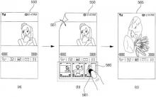
LG received a US patent (#8,271,047, applied to in 2008) that describes a mobile device interface that uses a bendable screen. LG's patented device uses two display - the top one is bendable while the bottom one is a rigid touch display. The user can bend or fold the top display to react with the device.

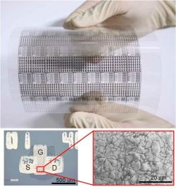
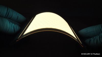
This seems to be a rather weird design. LG Display has plans to start mass producing flexible OLED panels in the second half of 2013, so such a device may see the light of day in the near future (although to be fair, these first flexible OLEDs will probably not be bendable).

Read the full story Posted: Sep 20,2012

Researchers develop a CNT based flexible display TFT array

Researchers from Japan developed a new flexible display TFT based on carbon nanotubes (CNT), using a flexographic printing technology in ambient temperature and pressure. The carrier mobility is as high as 112cm2/Vs. The flexographic technology, while lower in precision compared to gravure printing, has a high throughput - much higher than screen printing or ink-jet printing.

The researchers used silver (Ag) nanoparticles for gate electrodes and source/drain electrodes, imide resin for gate dielectric films and CNTs for the channel layer of the TFT. Oxygen plasma is used for the CNT patterning and a printing technology is used to form a resist layer for it.

Read the full story Posted: Sep 19,2012

China's Oasis New Energy embarks on a $500 million OLED project?

There's a report that CECEP Oasis New Energy signed an agreement with China's Suizhou district's government to build a new OLED fab with an annual capacity of 500,000 square meters. Total investment will be $500 million, and the company expects to reach an annual revenue of about $700 million.

We don't have any technical details about this new project, besides that the OLED panels will be use an a-Si backplane. Oasis NE is a solar PV developer and producer, based in Beijing, China.

Read the full story Posted: Sep 19,2012

Sumitomo to join the Holst Centre's flexible OLED lighting research

Sumitomo Chemical has joined the Holst Centre's shared research program on Printed Organic Lighting and Signage. The program's aim is to develop new manufacturing processes that enable low-cost flexible OLEDs. Sumitomo will help the program's investigation of multi-layer solution processes for high-efficiency OLEDs, using the company's PLED materials.

Flexible OLED lighting prototype

Sumitomo will provide other program members access to its OLED materials - especially the emitting materials. Sumitomo will be able to use the program's expertise in order to optimize its own materials for low-cost production and flexible substrates.

Read the full story Posted: Sep 19,2012

Fujifilm and Panasonic OLED EVFs - who's the microdisplay maker?

In the past few weeks several new digital cameras with OLED EVFs were announced: the Fujifilm X-E1, the panasonic GH3 and Sony's A99, NEX-6 and the RX-1. In the Sony cameras, the OLED microdisplays are made by Sony themselves. But who makes the other OLEDs used by Fujifilm and Panasonic?

The GH3's EVF has a microdisplay that sports 1,744k pixels - and that's all we know about it. Pocket-Lint claims that it sports an RGBB architecture (a second blue). This probably means that it is made by MicroOLED as we know they used this architecture (RGBB filters over white OLEDs) in their first-get WVGA OLED micodisplay, which fits the GH3 specification. UDC has also developed an RGBB architecture back in 2010, but it was a direct-emission design, so I don't think MicroOLED is using that design.

Read the full story Posted: Sep 19,2012

The NEMO project concludes, new soluble OLED materials developed

The three-year long NEMO (NEw Materials for OLEDs from solutions) project has been successfully concluded. Merck, the project's leader, says that the new soluble materials developed in the project can now be used in large-area OLED display and lighting panels. The new phosphorescent materials have an increased lifetime (200,000 hours for green) and efficiency (70 cd/A @ 1,000 cd/m2).

NEMO was a large €29 million project, co-funded by the German Federal Ministry of Education and Research (BMBF). The project's scope included emitter materials, charge transport materials and new adhesives for reliable encapsulation of each OLED component. The partners also performed physical tests on the materials and on the OLED components in order to gain more in-depth knowledge for future material developments.

Read the full story Posted: Sep 14,2012

UDC doesn't see more large acquisitions ahead

When Universal Display raised $250 million back in early 2011, they said they are looking at IP acquisition. Finally the company bought Fujifilm's OLED IP portfolio for $105 million in July 2012. During Deutsche Bank's dbAccess technology conference, UDC's CFO Sidney Rosenblatt revealed that when they raised the money they already had Fujifilm's portfolio in mind, and they didn't know what it would cost, so they raise $250 million.

Sidney further reveals that the company does not see any more large acquisitions ahead.

Read the full story Posted: Sep 14,2012

Sony's A99, RX1 and NEX-6 now available to order on Amazon

A few days ago Sony announced new cameras with OLED EVFs, and today they are available to buy on Amazon.com: The A99 for $2,798 (body only, will ship in October) and the NEX-6 for $848 (body only, will ship in November). The RX1 costs $2,798 (will ship in December, we do not know about the optional OLED EVF yet).

The A99 is Sony's flagship full-frame DLSR with a 24.7 mp sensor with on-sensor phase detection, dual AF system and Full-HD (1080p@60). The NEX-6 is a 16 mp mirrorless interchangeable lens camera that features Wi-Fi, in-camera apps and on-sensor phase detection.

Read the full story Posted: Sep 14,2012

Panasonic re-organizes to put more focus on OLED displays

According to a report from Nihon Keizai, Panasonic has taken steps to streamline its R&D and put more focus on OLED TV development. The company plans to invest ¥30 billion ($385 million) in a pilot AMOLED production line in Himeji (this was already reported in April). According to the report Panasonic wants to use PLEDs and ink-jet printing in its upcoming fab. Panasonic's P-OLED/Ink-jet development dates back to the OLED TV joint-venture with Sumitomo in 2009.

Sony OLED TV prototypeSony OLED TV prototype

The report also details the collaboration between Panasonic and Sony. The two companies have quite different technologies - Panasonic with its P-OLED and printing processes and Sony with small-molecules and VTE. It is claimed that Sony will mostly supply capital for Panasonic, and not technology. Sony's own OLED technology will be used though by Japan Display to make small sized panels.

Read the full story Posted: Sep 12,2012