What does the term ‘printed electronics’ mean?
Printed electronics refers to the production of electronics using soluble materials and printing technologies. Printed electronics is based on the combination of new materials and large area, high volume deposition and patterning techniques. A set of printing methods allow electronic and photonic devices to be printed using conductive or semiconductive inks and various substrates (mainly plastics and fabrics). Such methods may include screen printing, flexography, gravure, offset lithography and inkjet. These techniques may yield printed resistors, condensers, transistors and many other electronic components.

What are the advantages of printed electronics?
Printed electronics are considered easy to manufacture as well as cost-effective and time-saving, though mostly low-performance. The printed materials are usually very thin, light and flexible, and can be integrated into existing production lines for printed products. These advantages prove attractive to many existing applications, as well as inspiring for new applications.
What can printed electronics be used for?
Printed electronics is a growing field that opens the door to new possibilities, like smart containers and packages, fabrics that double as lighting fixtures, flexible screens and more. New applications are constantly becoming possible in consumer electronics, packaging, printing, automotive, medical/pharmaceutical industries and more.
Printed electronics technology is still in early stages: while increasing numbers of products are available, many applications are still in lab-scale development, prototype activities or early production. Printed electronics have already started to appear in our daily lives, for example in car manufacturing with printed aerials, smart textiles with pressure sensors to recognize seat occupancy and self-dimming rearview mirrors, or in the medical field with medical test strips with diagnostic electrodes.
Key trends in printed electronics are starting to become apparent, such as the rapid increase in the mobility of organic semiconductors, conductivity of printed conductors and efficiency of OPV materials, scaling down of patterning processes, development of flexible, lightweight, mobile electronic products enabled by organic electronics and early appearances of intelligent packaging and smart textiles applications.
Applications can be roughly divided into five main clusters:
- OLED Lighting
- OLED displays (mostly Flexible ones)
- Printable, Organic Photovoltaics (OPV)
- Electronics and Components (printed memory and batteries, active components and passive components)
- Integrated Smart Systems (ISS, including smart objects, RFID, sensors and smart textiles)

What materials can be used for printed electronics?
Material properties have a large impact on the differences between printed and conventional electronics. Printable materials grant major advantages in addition to printability, like mechanical flexibility and functional adjustment by chemical modification.

Inks used for printed electronics (that function as conductors, semiconductors, dielectrics, or insulators) are required to be in liquid form, for solution, dispersion or suspension. Materials for printed electronics can be of organic as well as inorganic nature. Most inorganic ink materials are dispersions of metallic or semiconducting micro and nano-particles. Semiconducting nanoparticles include silicon and oxide semiconductors. Silicon is also printed as an organic precursor which is then converted by chemical processes into crystalline silicon.
Inorganic electronics demonstrate ordered layers and interfaces that organic and polymer materials cannot provide. Silver nanoparticles are used in several printing methods, including offset and inkjet (gold particles are also used in inkjet).
Organic printed electronics integrate knowledge and methods derived from printing, electronics, chemistry (especially from organic and polymer chemistry). Organic materials in part differ from conventional electronics in terms of structure, operation and functionality, which influence device and circuit design and optimization as well as fabrication method. Conductive inks are often used for printing electronics; These inks contain components that provide the function of conductivity and may be comprised of silver, carbon, graphite, or other precious metal coated base material. Graphene, a unique form of carbon, make for especially interesting conductive inks with extraordinary properties.
Printed electronics enable the use of flexible substrates, which lowers production costs and allows fabrication of flexible circuits. Paper's low costs and manifold applications make it an attractive substrate, however, its high roughness and large absorbency make it problematic for electronics. Other common flexible substrates are polyimide films and various types of plastic and steel films.
What are OLEDs?
OLED (Organic Light Emitting Diodes) is a flat light emitting technology, made by placing a series of organic thin films (usually carbon based) between two conductors. When an electrical current is applied, light is emitted. OLEDs can be used to make displays and lighting, with possible applications that span TV sets, computer screens, mobile phones, decorative lighting and more. Since OLEDs emit light they do not require a backlight and so they are thinner than LCD displays, and are also more efficient, simpler to make and boast a better color contrast.
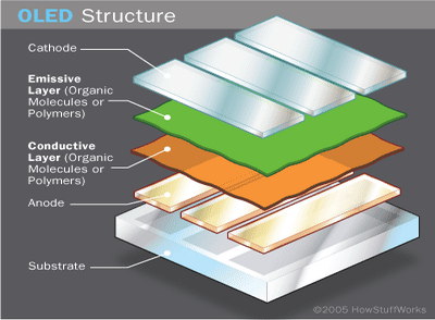
An OLED 'light bulb' is a thin film of material that emits light. OLEDs provide an area-lighting panel (rather than point-lighting provided by LEDs) and feature good color temperature. In fact some OLEDs are color tunable. OLEDs can also be made flexible or transparent - and in the future we can expect exciting new luminaire design that use those advanced panels.
Printed electronics and OLEDs
A common viewpoint regards OLED technologies as part of the printed electronics industry. This is, however, a misconception as almost all OLED panels today are not actually produced using printed technologies (but rather through vapor evaporation). Interestingly, people usually estimate the printed-electronics market at around $20 billion (yearly revenue). Out of that, about $15 billion represent OLED panel sales - even though the vast majority of those OLEDs do not use printed processes at allâ¦
Printing OLED panels is indeed possible - or at least printing some of the (many) layers that comprise an OLED panel is entirely possible. Many people consider ink-jet printing (and nozzle-printing) technologies to be the leading next-gen OLED deposition technology, as these kinds of processes can produce large-area OLED panels quickly and efficiently. Currently there is no commercial production of OLED displays performed using such techniques.
OLED lighting can also be produced using soluble OLED materials and printing technologies, and these technologies can be very useful to lower production costs, and are especially suited for lighting as there's no patterning required.