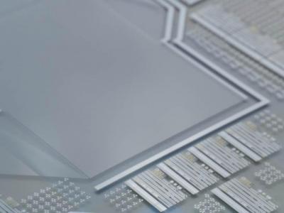
Researchers from the Holst Centre developed a new process to deposit semiconductor layers with better performance and high throughput than PVD-based process. the new process is based on scalable, atmospheric-pressure process spatial-ALD.

The Holst Centre used sALD to deposit IGZO backplanes that achieved charge carrier mobilities of 30 to 45 cm2/Vs. The researchers say that similar backplanes deposited with PVD (supttering) achieve about 10 cm2/Vs. The sALD layers also exhibited low off current, switch-on voltages around 0 V and excellent bias stress stability.
The Holst Centre are now looking into scaling up and commercialization of the new process.
Posted: Nov 24,2016 by Ron Mertens

